Si deseas distinguir tus productos, servicios o ambos de los de otra empresa, es posible que necesites una marca o nombre comercial. Descubre qué son, en qué consiste su procedimiento de registro y qué implica.

Información sobre los plazos de presentación de solicitudes de transformación de marcas de la Unión Europea en marca nacional española. Más información


Si tienes un nuevo dispositivo, producto o procedimiento que resuelva un problema técnico o tenga una ventaja práctica, existen distintas formas de protegerlo en España y en otros países. Descubre cómo hacerlo.

¿Tu innovación reside en la estética, la ornamentación o la apariencia de tu producto? Protégela mediante un diseño industrial. Descubre qué derechos confiere el registro y cómo realizar la tramitación.

Las indicaciones geográficas protegen el nombre de un producto originario de una zona geográfica, a la cual le debe una determinada calidad, reputación u otra característica. Descubre qué son, en qué consiste su procedimiento de registro y qué beneficios conceden.

Las patentes publicadas en todo el mundo son una valiosa fuente de información científica, técnica y comercial.

Si eres emprendedor/a o una empresa y quieres potenciar y mejorar la rentabilidad de tu negocio protegiendo de forma adecuada los activos intangibles de tu organización, en este espacio encontrarás lo necesario.


 161
resultados
161
resultados
 Última actualización
15/09/2026 [08:03:00]
Última actualización
15/09/2026 [08:03:00]


 Resultados 75 a 100 de 161

Resumen de: WO2025097037A1
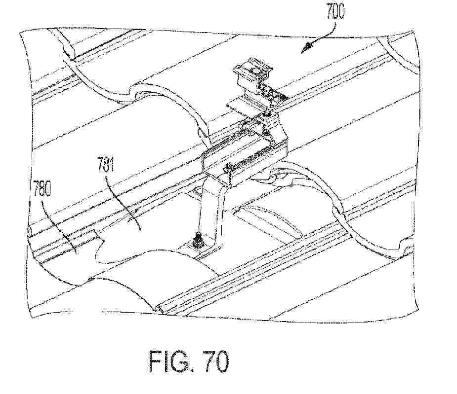
A roof mount (700) includes a base assembly installable on a roof including a foot (703), an arm (705), and a slider (707). A flashing (780) is positioned between the foot (703) and the arm (705) and an adjustment assembly (704) is coupled to the slider (707). The adjustment assembly (704) includes a partially threaded shaft (706), an adjustment nut (708), and a support nut (710). A clamp (712) is adjustably connected to the base assembly by the adjustment assembly (704) and a distance between the clamp (712) and the slider (707) is adjustable. The clamp (712) includes a first clamp portion (714) and a second clamp portion (726). The first clamp portion (714) includes a central portion (716), a first support surface (718), and a second support surface (720). The central portion (716) is disposed between the first support surface (718) and the second support surface (720). A first fastener (728) is connected to the clamp (712) and operable to tighten the second clamp portion (726) to the first clamp portion (714). A roof mount system includes a roof mount (700) and at least one skirt (400).

Resumen de: EP4804764A1
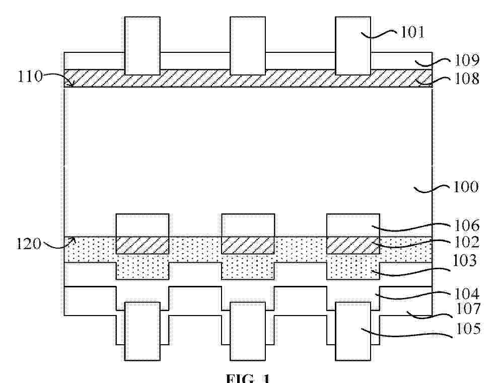
0001 Embodiments of the present disclosure relate to the field of photovoltaic technology, and provide a solar cell and a method for producing the same. The solar cell includes: a substrate including a front surface and a back surface opposite to each other, front electrodes formed on the front surface, at least one doped structure formed on the back surface and having doping ions of a first type, a tunneling layer covering at least portions of the back surface and a surface of the at least one doped structure away from the substrate, a doped conductive layer formed over a surface of the tunneling layer away from the substrate and having doping ions of a second type, and back electrodes formed on a side of the doped conductive layer away from the substrate and in electrical connection with the doped conductive layer. The first type is one of N type and P type, and the second type is the other one of N type and P type.
Resumen de: EP4803164A1
The invention discloses a power generation device, method, and communication system that incorporate multimode communication, AI technology, and security monitoring.The invention generates a continuous supply of electrical energy through an alternative power generation approach, thereby avoiding the impact of environmental factors on battery performance and ensuring a stable power supply.
Resumen de: EP4804400A1
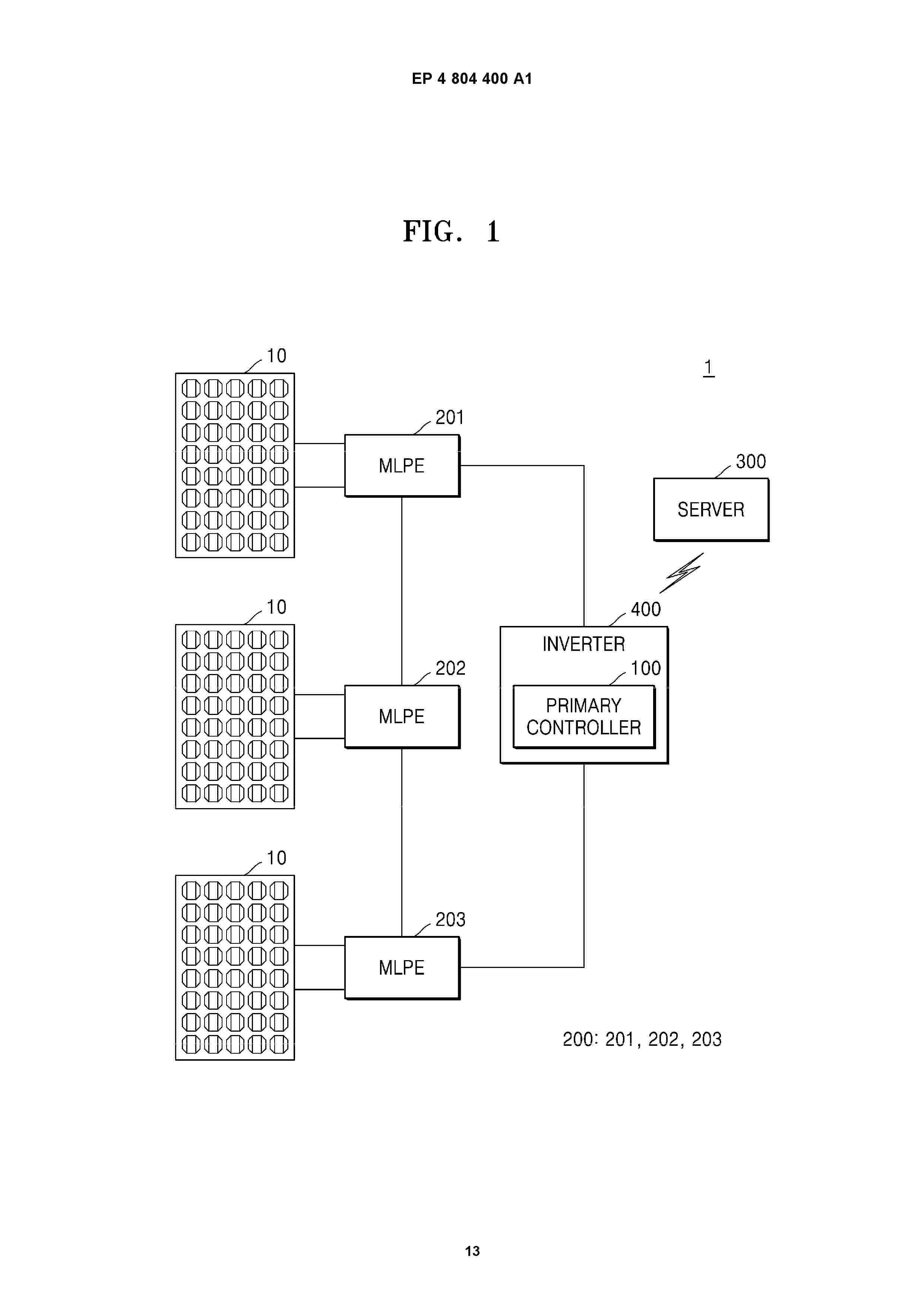
Disclosed is an inverter and a primary controller of a photovoltaic (PV) power generation system, and an operation method of the system. The operation method of the PV power generation system is an operation method performed by the primary controller of the PV power generation system, and the operation method may include: generating a plurality of operation signals having different signal levels; periodically transmitting the plurality of operation signals to a plurality of module level power electronics (MLPE) connected to a plurality of PV panels; and receiving a response signal for an operation signal from at least one MLPE that has received at least one of the plurality of operation signals transmitted periodically, and controlling signal levels of the plurality of operation signals based on a result of reception of the response signal.
Resumen de: CN122122798A
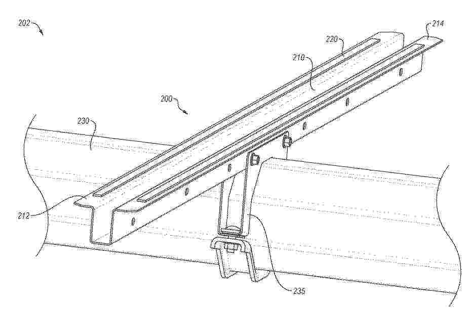
A field photovoltaic (PV) module assembly system and process may involve customizing the assembly of a row of PV modules at a location of a specific solar site. A mounting rail or other mounting structure configured to engage the PV module with the torque tube may be positioned in-situ along the torque tube to account for physical characteristics and attributes of a particular solar field. The PV module may be attached to one or more mounting rails by an adhesive. Attachment of the PV module to the mounting rail using an adhesive may increase the flexibility of mounting the PV module along the torque tube. The use of the adhesive may also reduce the number of fastening components, such as structural rails or module rails, included in the mounting rails and PV modules.
Resumen de: PL451360A1
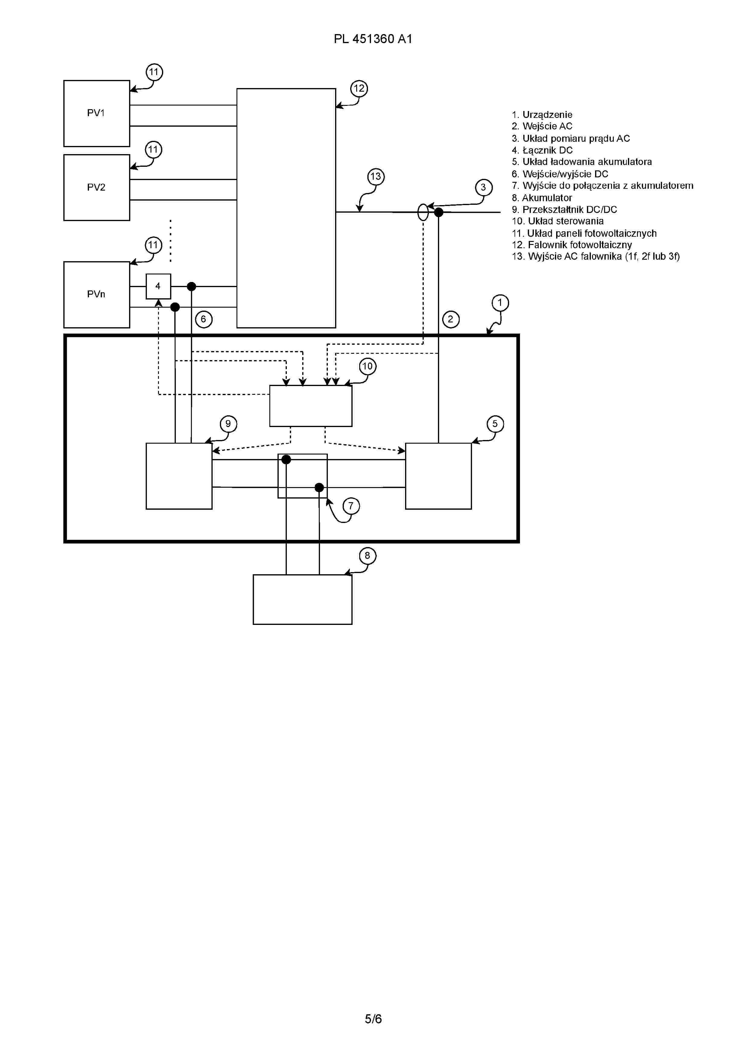
Przedmiotem zgłoszenia jest urządzenie do włączenia magazynu energii w instalacje fotowoltaiczne typu on-grid oraz instalacja fotowoltaiczna. Urządzenie (1) zawierające co najmniej jedno wejście AC (2) jedno, dwu lub trzyfazowe, układ pomiaru prądu AC (3), układ ładowania akumulatora (5), przynajmniej jedno wejście/wyjście DC (6), przekształtnik DC/DC (9), układ sterowania (10), wyjście do połączenia z akumulatorem (7) charakteryzuje się tym, że wejście AC (2) urządzenia (1) jest połączone z wejściem AC układu do ładowania akumulatora (5), układ do ładowania akumulatora (5) jest przekształtnikiem AC/DC i jego wyjście DC jest połączone z wyjściem do ładowania akumulatora (7) lub bezpośrednio z akumulatorem (8) oraz z wejściem DC przekształtnika DC/DC (9), wyjście przekształtnika DC/DC (9) jest połączone z wejściem/wyjściem DC (6) urządzenia (1), układ pomiaru prądu AC (3) oraz wejście AC (2) i wejście/wyjście DC (6) są połączone z układem sterującym (10), wyjścia układu sterującego (10) są połączone z przekształtnikiem DC/DC (9) oraz układem do ładowania akumulatora (5).
Resumen de: PL451393A1
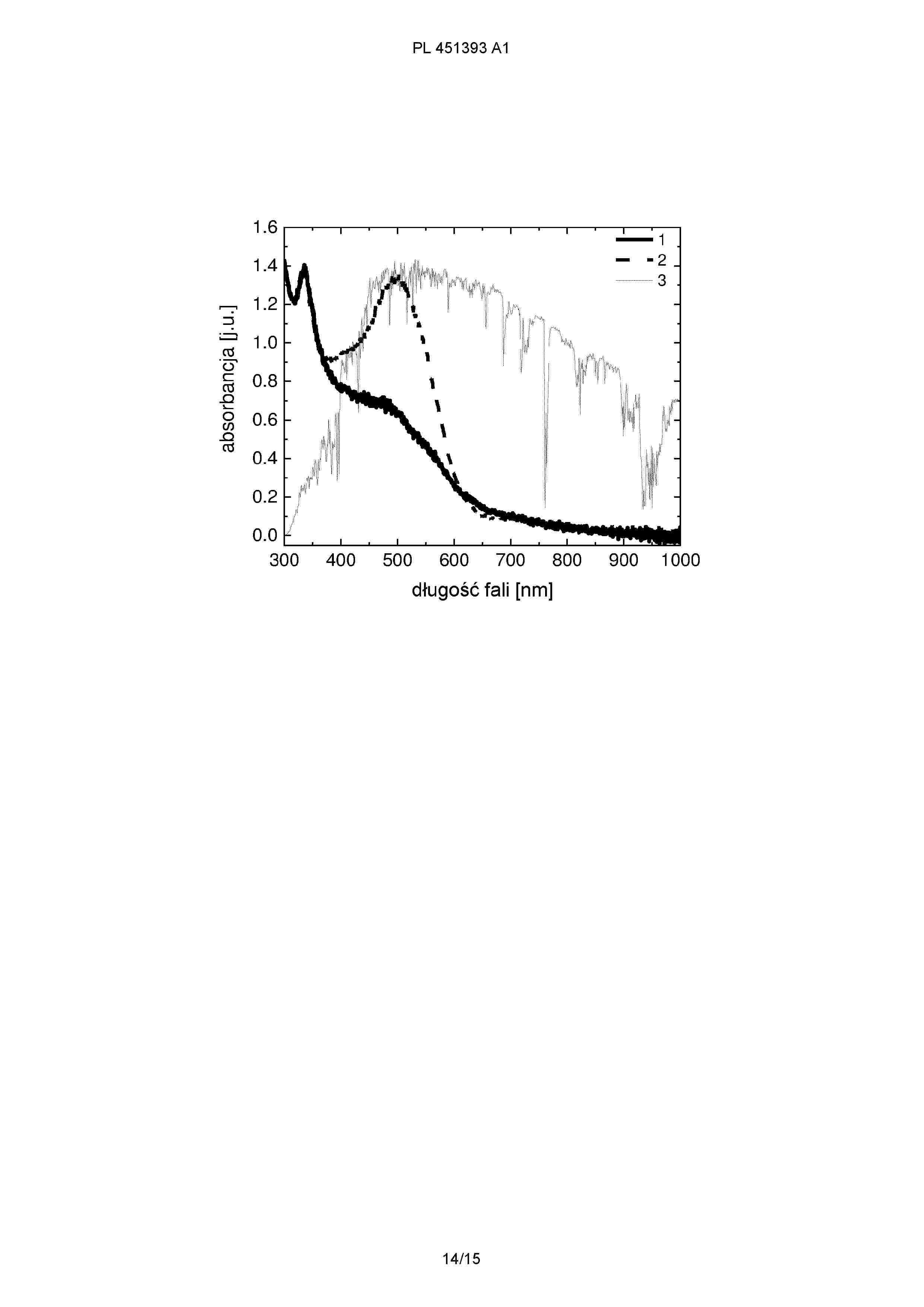
Organiczne ogniwo fotowoltaiczne zawiera warstwę aktywną o wysokiej absorbancji promieniowania słonecznego, umieszczoną pomiędzy górną elektrodą transparentną z ITO o grubości 100 - 130 nm i oporności powierzchniowej 7 - 15 Ů/sq, osadzoną na podłożu o grubości 0,6 - 1 cm oraz elektrodą dolną z AI o grubości 120 - 160 nm. Warstwa aktywna ma grubość 60 - 110 nm i zawiera poli(3-heksylotiofen) (P3HT) stanowiący donor 1, ester metylowy kwasu 6,6-fenylo-c71 -masłowego (PCBM) stanowiący akceptor oraz kwas 2-cyjano-3-4-4-(2,2-difenyloetenylo)fenylo-1,2,3,3a,4,8b-heksahydrocyklopentbindol-7-ylo-2-propenowy (Dye131) stanowiący donor 2. Stosunek wagowy sumy składników donorowych P3HT i Dye131 do składnika akceptorowego PCBM wynosi 1:1, a ilość każdego pojedynczego składnika w postaci P3HT lub Dye131, w sumie składników donorowych wynosi od 44% do 56% wagowych. Sposób wytwarzania organicznego ogniwa fotowoltaicznego polega na rozpuszczeniu osobno P3HT, Dye131 i PCBM, w ilości 10 mg/µl każdy, ich wymieszaniu i naniesieniu metodą spin-coatingu w atmosferze argonu na górną elektrodę transparentną w postaci oczyszczonego podłoża z ITO, a w końcowym etapie naparowaniu elektrody dolnej z AI.
Resumen de: FR3172702A1
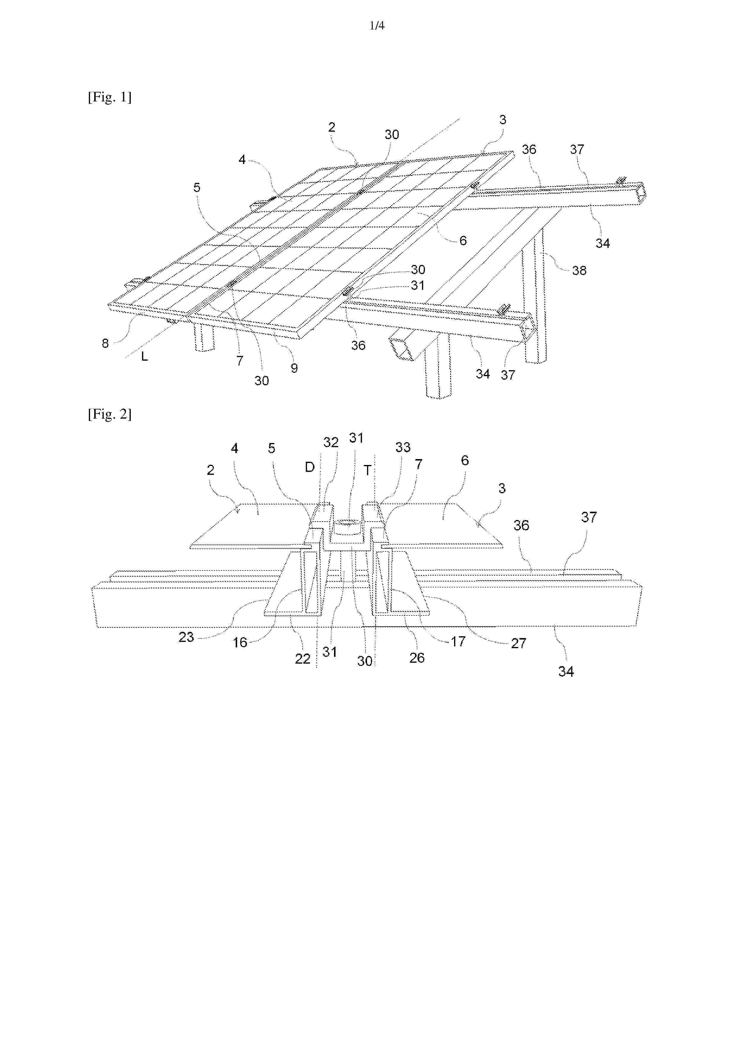
Dispositif de fixation de panneaux solaires à un bâti, système de fixation et ensemble de conversion du rayonnement solaire associés. - L’invention concerne un dispositif de fixation (1) à un bâti (38) de deux panneaux solaires (2, 3) adjacents et comprenant chacun une plaque (4, 6) formant capteur solaire et un longeron de support (5, 7) attaché à cette dernière, comprenant : une première et une deuxième mâchoire (10, 11),un moyen d’ajustement (12) conçu pour refermer lesdites première et deuxième mâchoires (10, 11) l’une vers l’autre afin qu’elles enserrent les deux longerons (5, 7) entre elles, verrouillant ainsi en position lesdits deux longerons (5, 7) l’un par rapport à l’autre. - Le dispositif de fixation (1) selon l’invention est particulièrement destiné au maintien d’un panneau solaire (2) sur un bâti (38) même en cas de vent violent. Figure 3.
Resumen de: WO2026182334A1
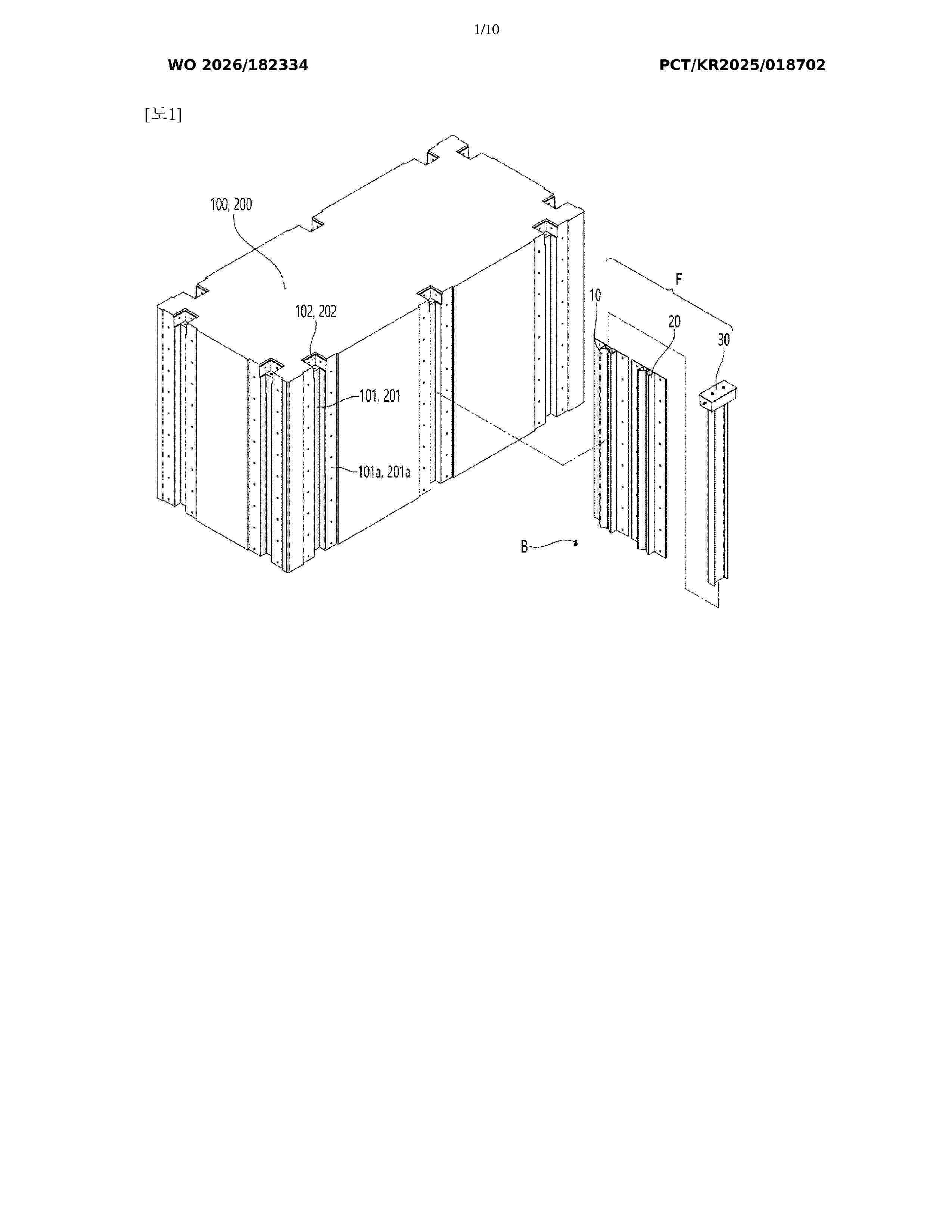
The present invention relates to a coupling device for floating bodies, and a floating body coupling assembly using same. Disclosed are the coupling device for floating bodies, and a floating body coupling assembly using same, according to one aspect of the present invention, the coupling device coupling a plurality of floating bodies having a rectangular parallelepiped shape together in a side-by-side manner in order to provide a large device such as a floating solar power substation on the water.
Resumen de: US20260261231A1
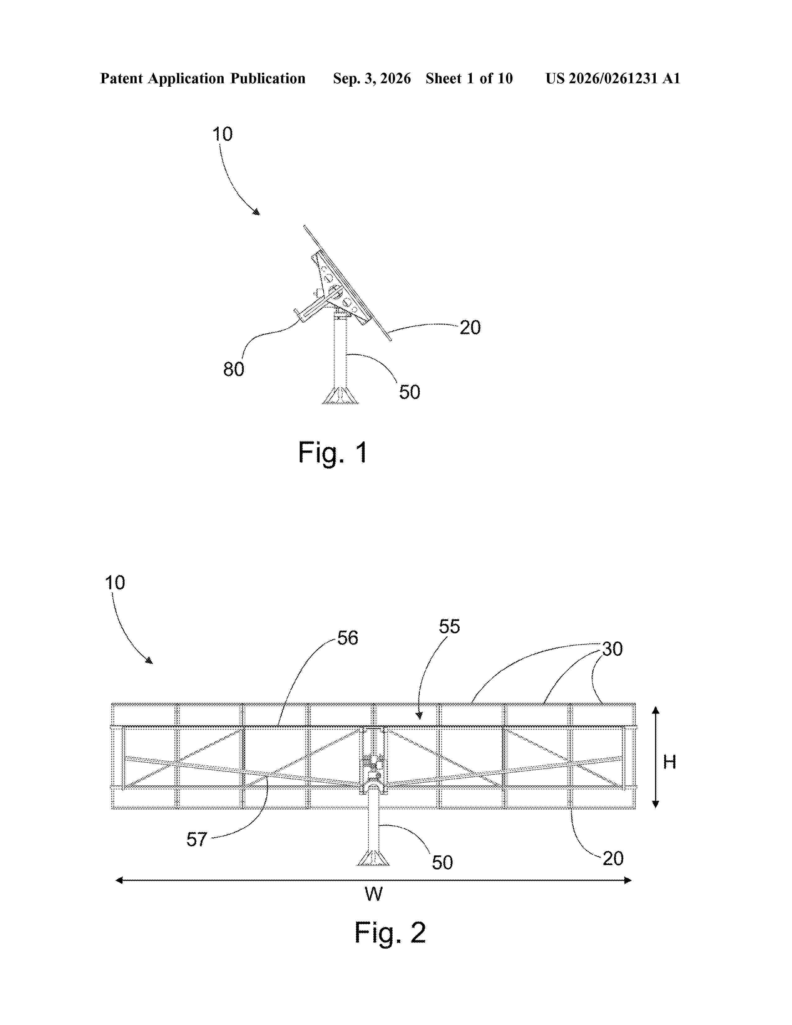
A system for producing electricity with solar panels includes solar panel systems arranged in a grid formation, wherein each solar panel system includes a solar cell assembly consisting of solar panels configured to be movable on a support structure. A connection of each solar cell assembly includes rotation means and tilting means. The system includes control means by means of which, at a selected moment in time, when an incoming angle of the sun's rays is greater than a selected minimum value, but less than a selected limit value, the solar cell assemblies are configured to be rotated so that an angle of rotation of the solar cell assemblies relative to the direction of incoming sunlight is 20°-50°, andtilted to reduce a three-dimensional solar incidence angle of the solar cell assemblies so that the solar cell assemblies do not overshadow one another.
Resumen de: US20260261141A1
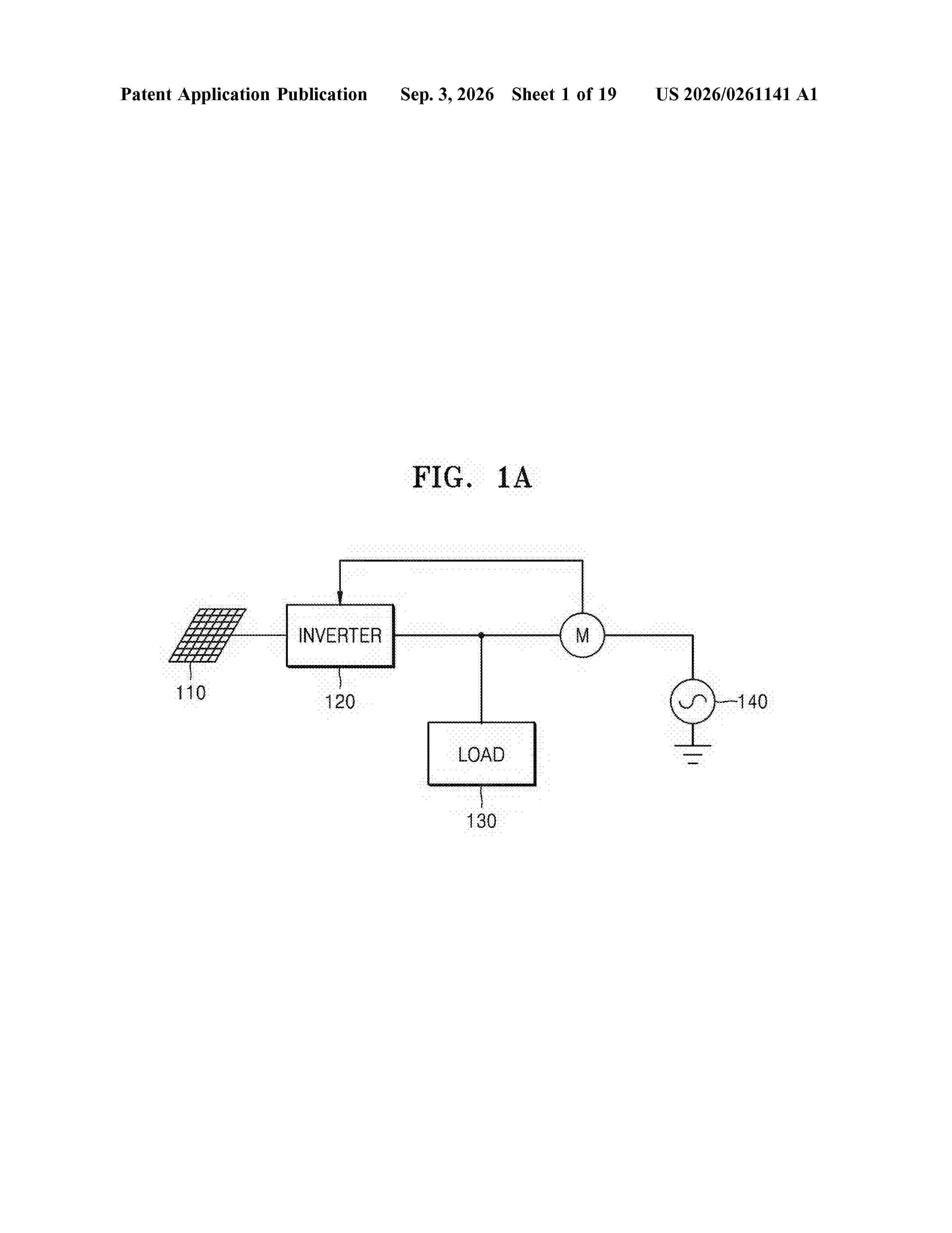
0000 A photovoltaic system according to an embodiment of the present disclosure includes an energy storage system (ESS) that is communicatively connected and controllable, at least one distributed energy resource (DER) that is optionally connected, and a backup device configured to control a supply and backup of power to a load connected thereto, wherein the backup device may include a main relay, a load relay, and a processor configured to control the main relay and the load relay to perform the on- or off-operation based on at least one of whether the power grid is interconnected, and an available output power and a charging state of the energy storage system, and control at least one of the power grid, the energy storage system, and the distributed energy resource to supply power to the load based on the operations of the main relay and the load relay.
Resumen de: US20260262324A1
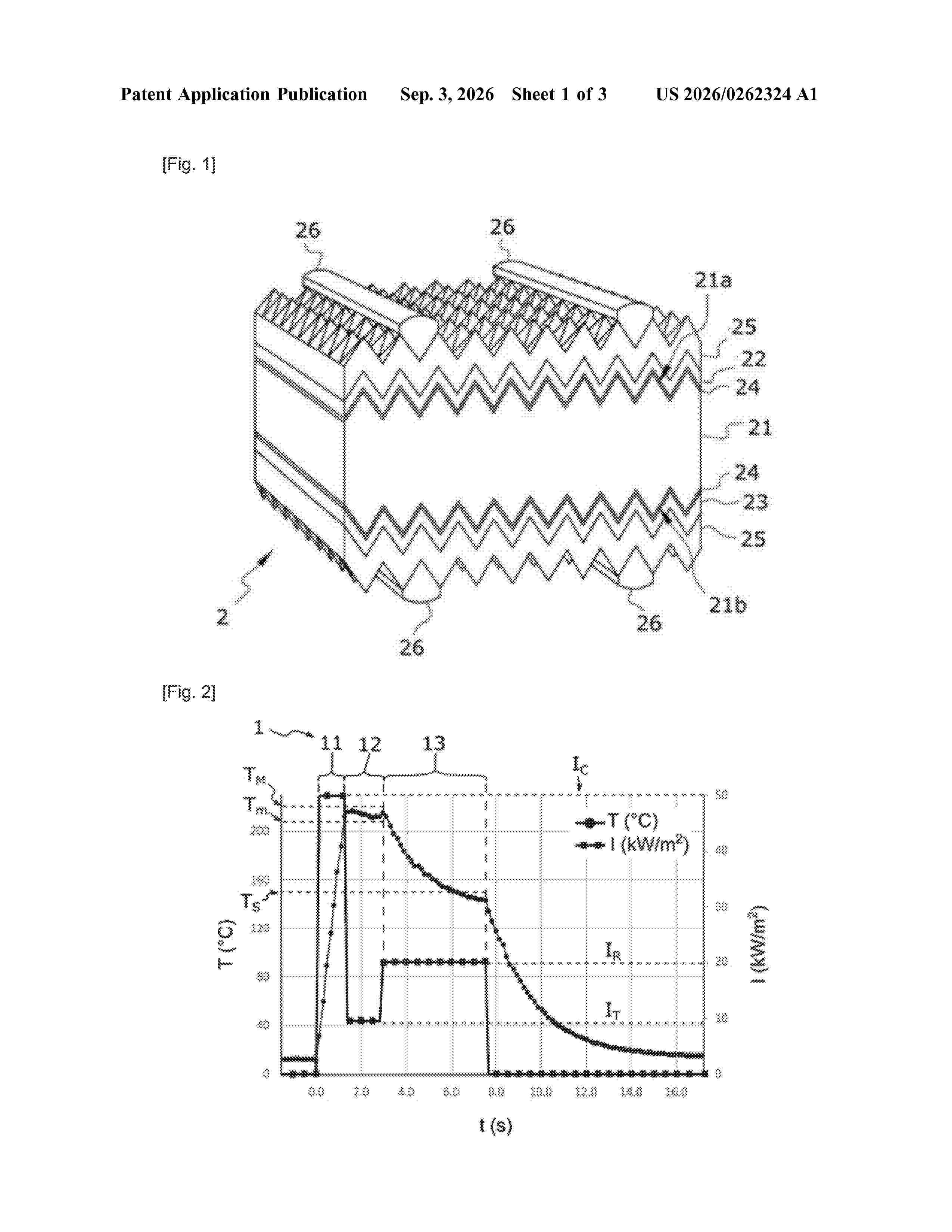
0000 A method for improving conversion efficiency of a photovoltaic cell includes treating the cell by exposing it to electromagnetic radiation having a treatment irradiance; and cooling the cell until its temperature reaches a threshold temperature, the exposure of the cell to electromagnetic radiation being maintained and the cooling irradiance of the electromagnetic radiation being greater than or equal to the treatment irradiance.
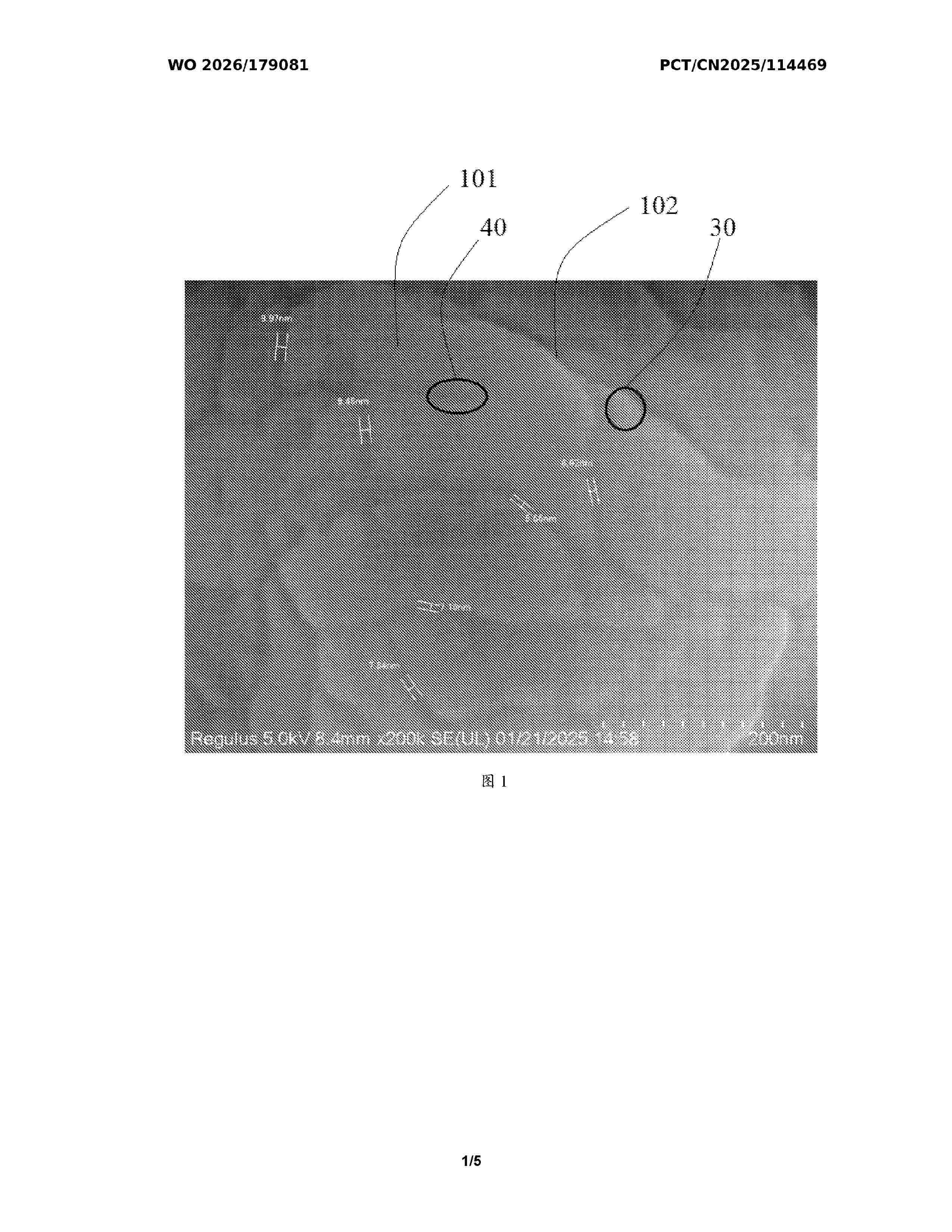
Resumen de: WO2026179081A1
The present disclosure provides a cell, a module, and a photovoltaic system. The cell comprises: a silicon substrate comprising a first region and a second region, wherein the first region is provided with a P-type polysilicon layer comprising a plurality of P-type crystal grains, the second region is provided with an N-type polysilicon layer comprising a plurality of N-type crystal grains, and the undulation degree of the P-type crystal grains is greater than that of the N-type crystal grains.
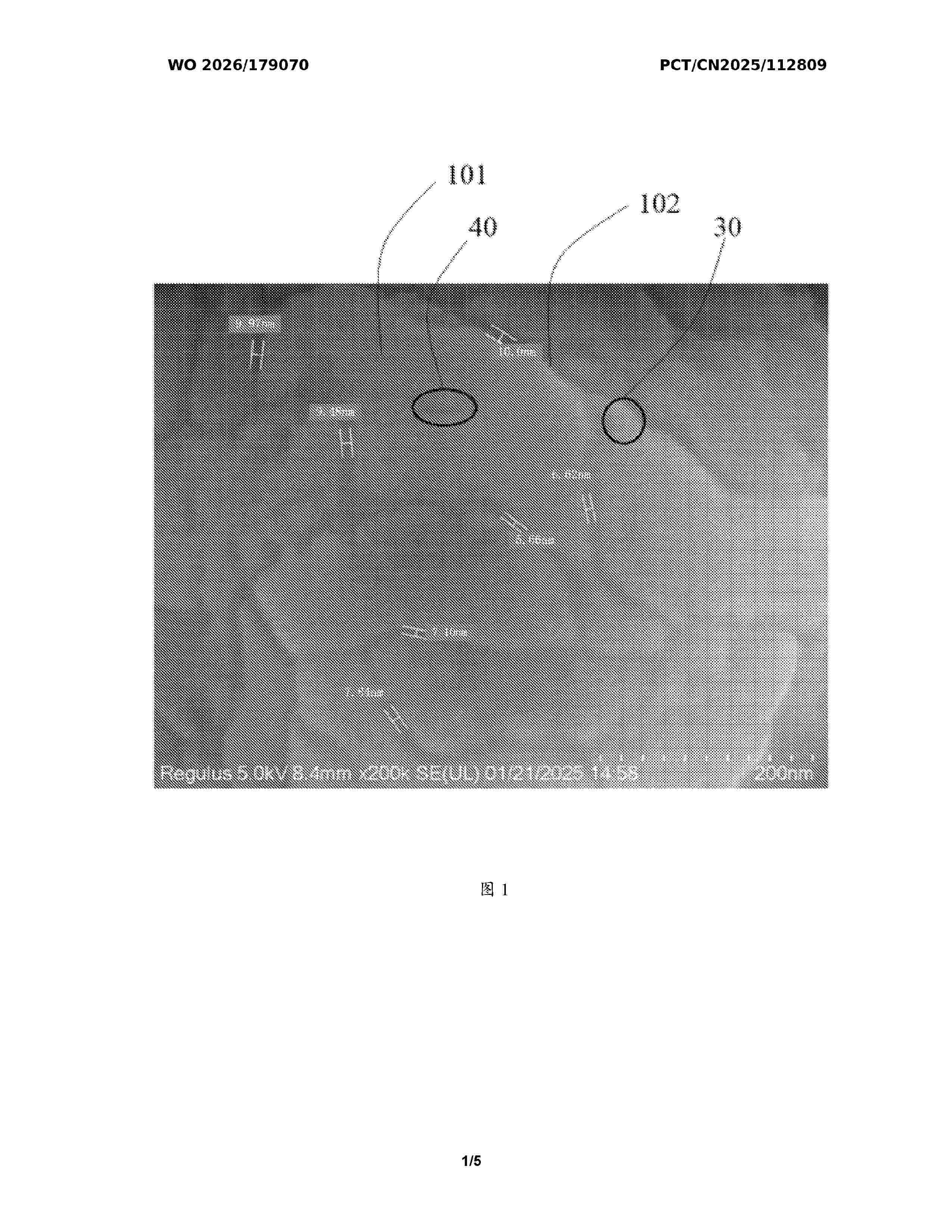
Resumen de: WO2026179070A1
The present disclosure is applicable to the technical field of photovoltaics. Provided are a cell, a module, and a photovoltaic system. The cell comprises: a silicon substrate, which comprises a first region and a second region, wherein a P-type polycrystalline silicon layer comprising several P-type grains is disposed in the first region, and an N-type polycrystalline silicon layer comprising several N-type grains is disposed in the second region. Separation and collection of holes and electrons are facilitated, and the transport efficiency of the cell is improved.
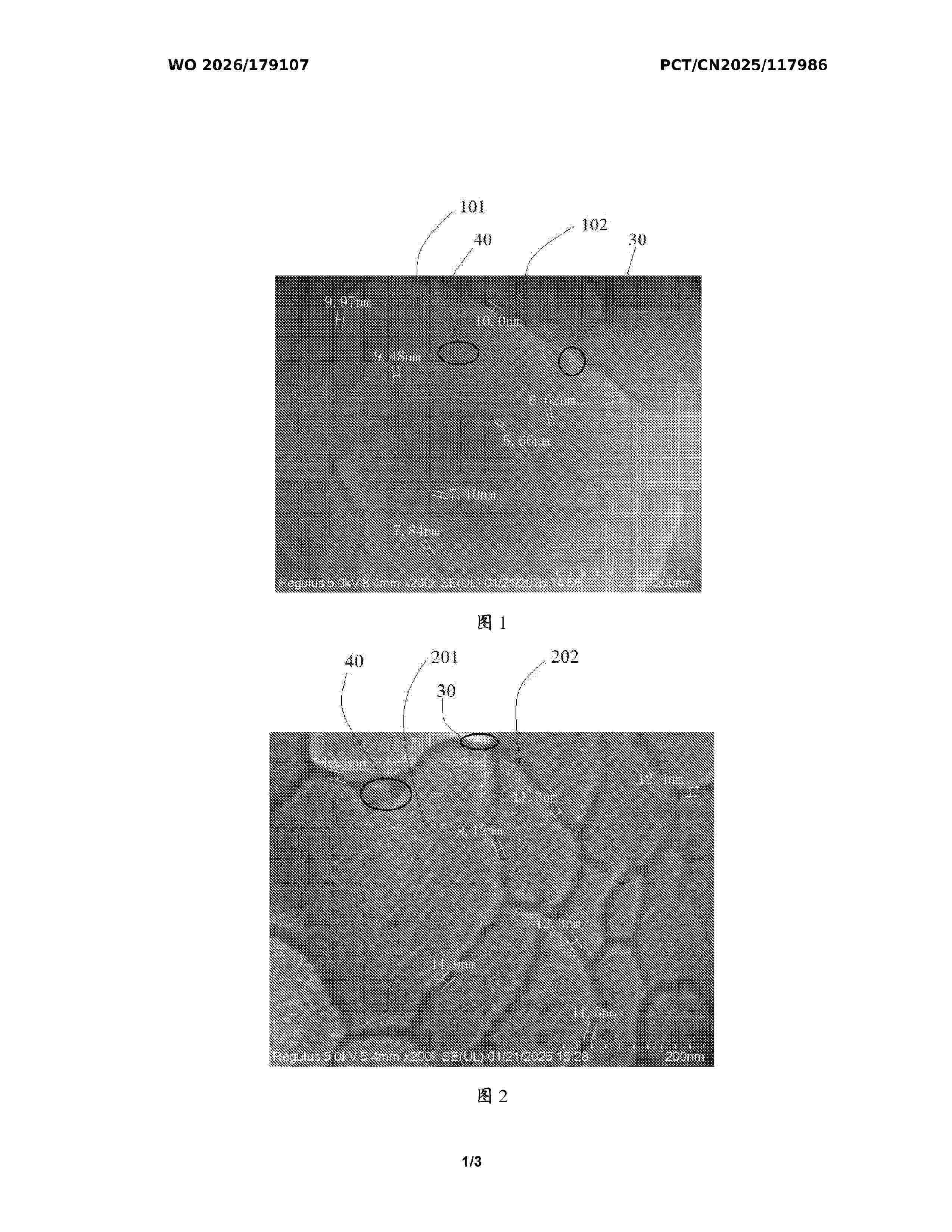
Resumen de: WO2026179107A1
In the photovoltaic cell of the present disclosure, a P-type polycrystalline silicon layer is provided in a first region of a silicon substrate, and an N-type polycrystalline silicon layer is provided in a second region of the silicon substrate. The P-type polycrystalline silicon layer comprises multiple P-type crystal grains, and a first grain boundary is formed between every two adjacent P-type crystal grains; the N-type polycrystalline silicon layer comprises multiple N-type crystal grains, and a second grain boundary is formed between every two adjacent N-type crystal grains; and the width of the first grain boundary is smaller than the width of the second grain boundary.
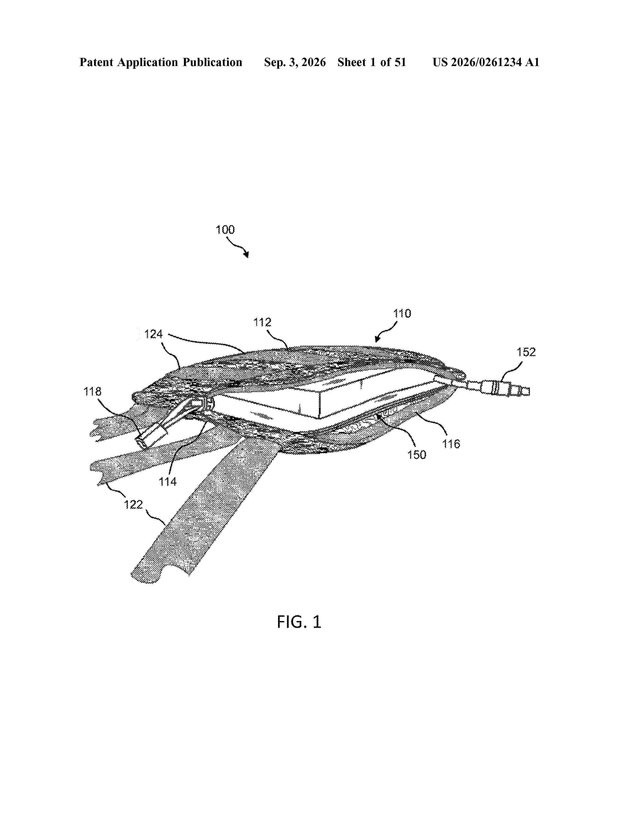
Resumen de: US20260261234A1
0000 A foldable solar panel including at least two solar modules mounted to a substrate. The foldable solar panel includes hook and loop tape to secure the foldable solar panel in the folded configuration. The foldable solar panel includes at least two straps and at least two horizontal rows of webbing operable to attach the foldable solar panel to a load-bearing platform.
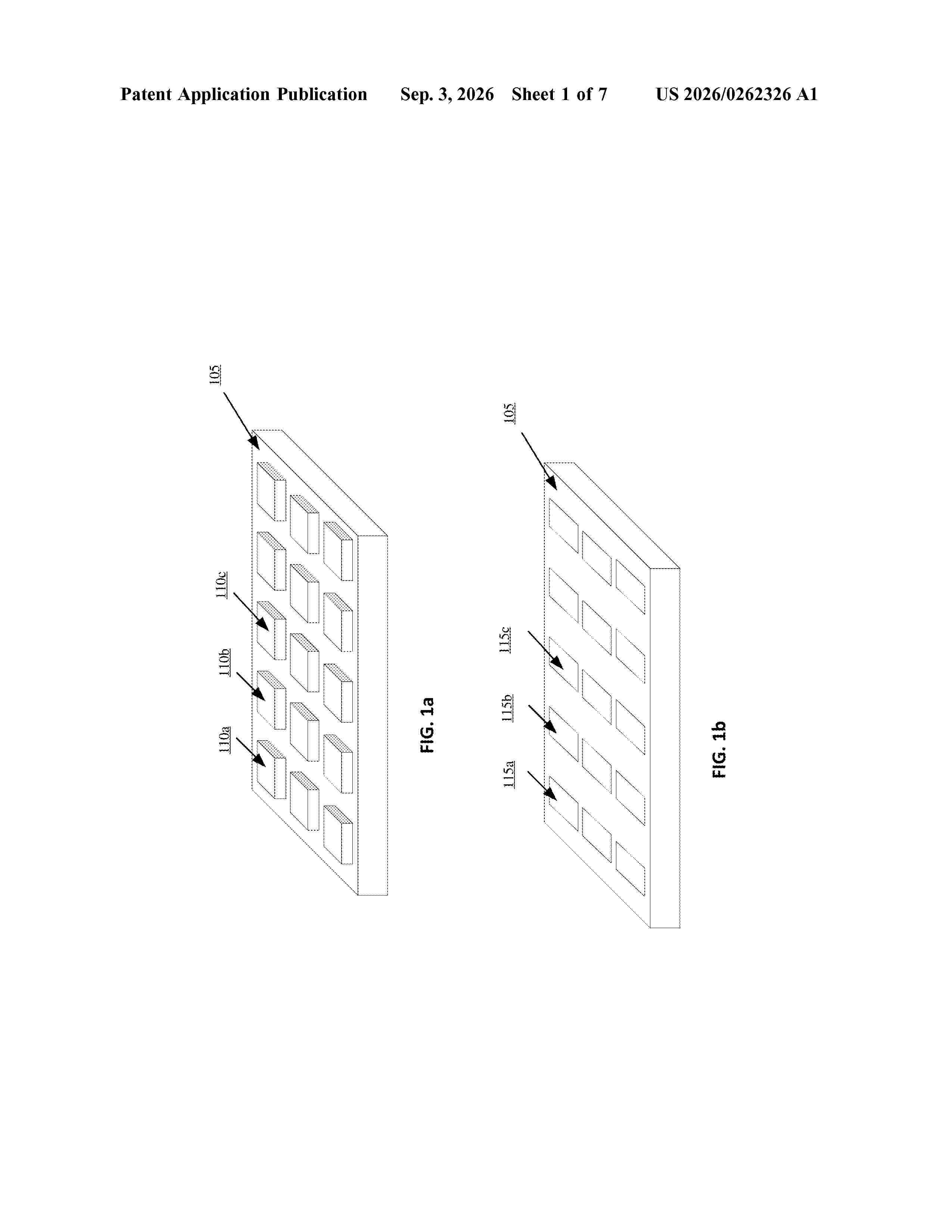
Resumen de: US20260262326A1
0000 A solar cell device and a method of making the same are provided. The method of making a solar cell device includes inkjet printing microdots on a substrate, dewetting the microdots to obtain nanoparticles at positions where the plurality of microdots were printed, depositing a thin film on the nanoparticles, and dewetting the thin film to form nanorods and nanoparticles on the same surface, wherein the positions of the nanoparticles on the surface of the substrate serve as seeds for the formation of the nanords.
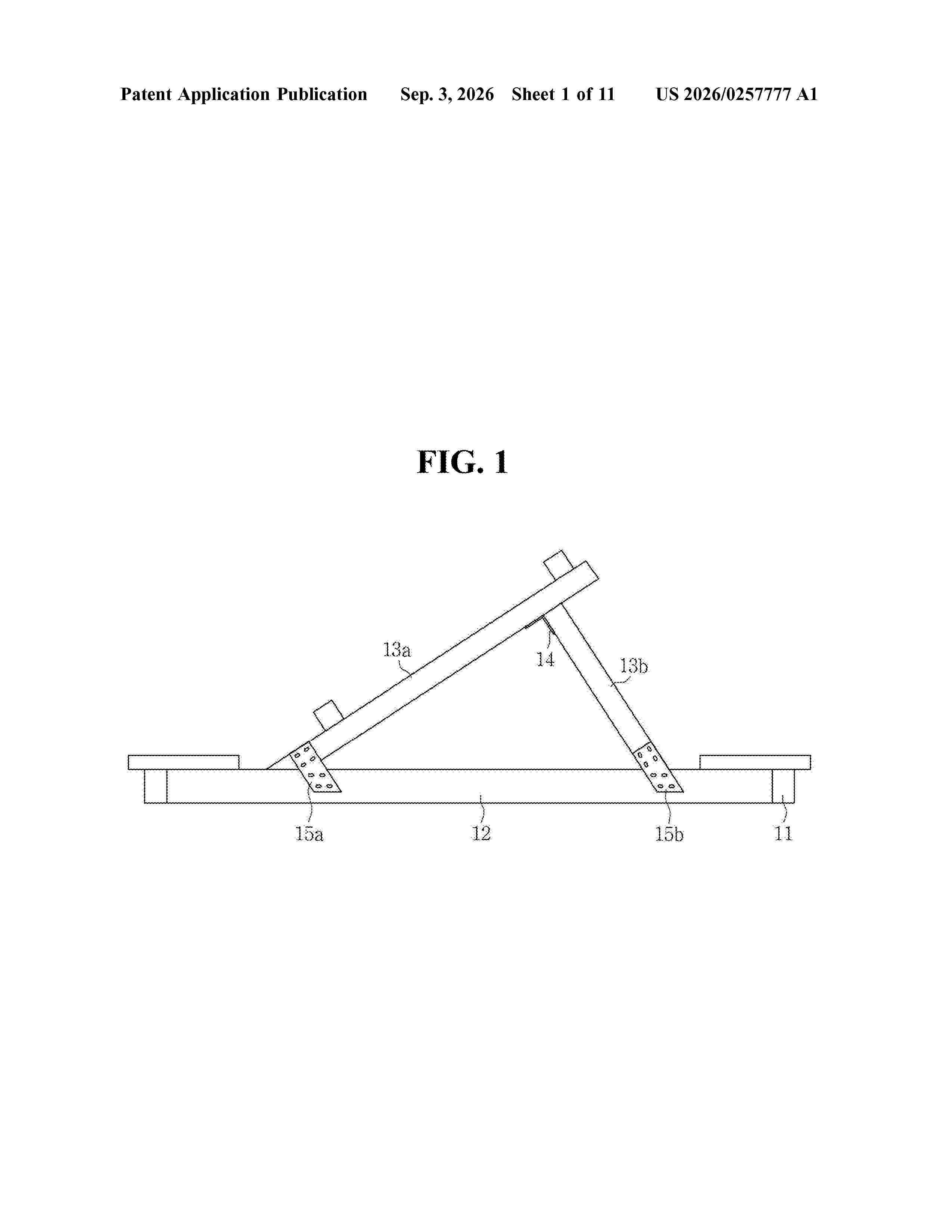
Resumen de: US20260257777A1
A solar panel tilt support member for a floating solar power generation apparatus, includes: a lower fixing part elongated in the front-rear direction and fixed to a longitudinal or transverse horizontal frame; an inclined support part extending rearward and obliquely upward from the front end of the lower fixing part to support upper and lower transverse support frames holding the solar panel; and a rear end support part extending upward from the rear end of the lower fixing part and joined with the inclined support part to form a triangular structure with the lower fixing part. A pair of tilt support members are disposed side by side to support the solar panel.
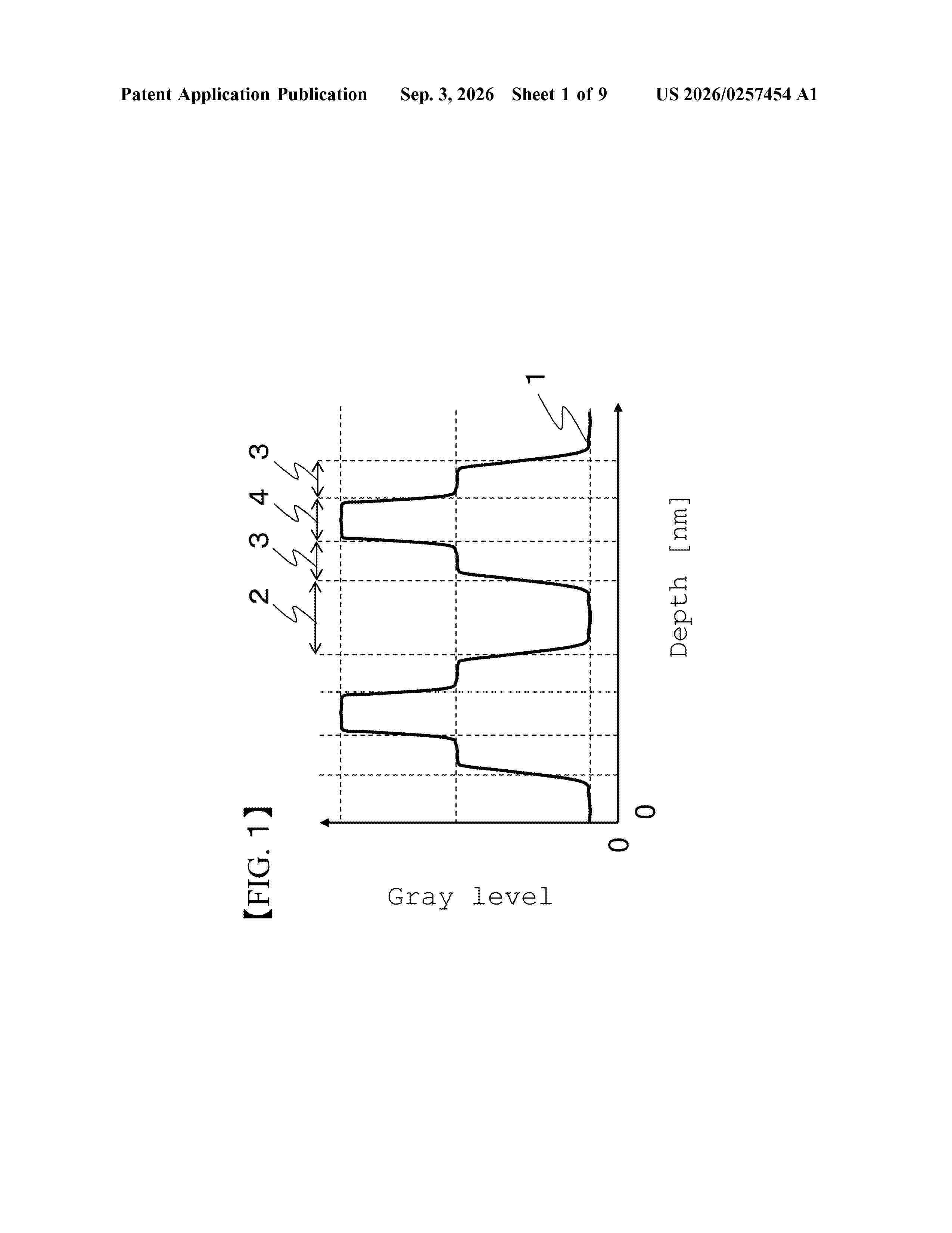
Resumen de: US20260257454A1
The present disclosure provides a laminated film including three or more ordered arrays composed of thermoplastic resin layers of three different types.
Resumen de: WO2026179196A1
The present disclosure provides a photovoltaic cell, module, and system. A P-type polysilicon layer in a first region of a silicon substrate comprises a plurality of P-type grains, and an N-type polysilicon layer in a second region of the silicon substrate comprises a plurality of N-type grains. The number of protruding P-type grains per unit area in the first region is less than the number of protruding N-type grains per unit area in the second region.
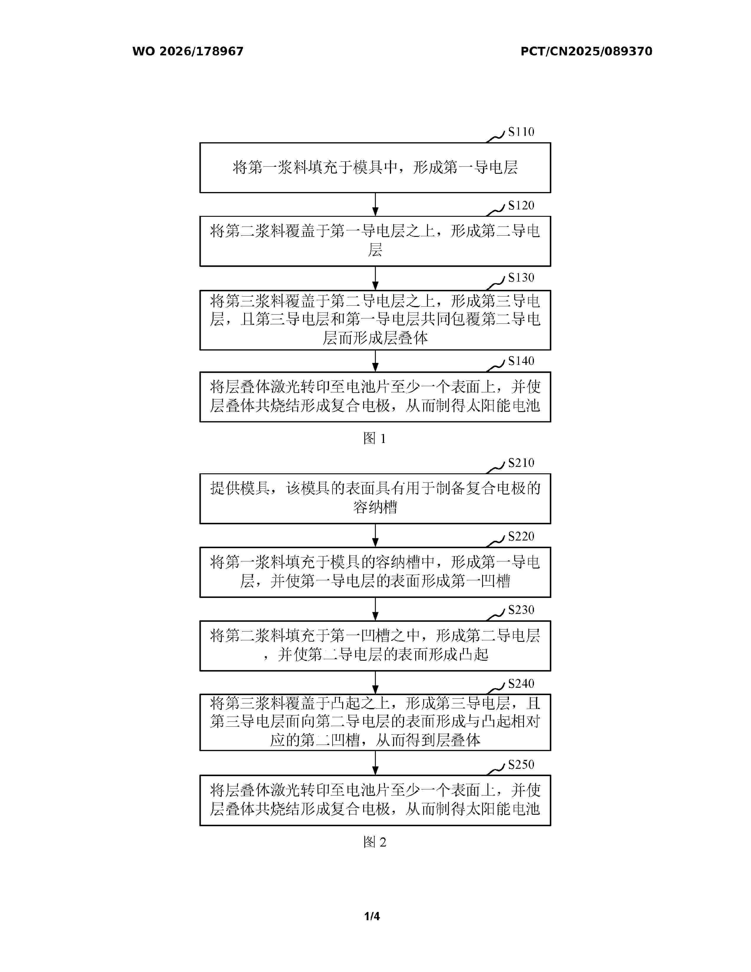
Resumen de: WO2026178967A1
The present application relates to a solar cell and a preparation method therefor. The method for preparing a solar cell comprises the following steps: filling a mold with a first slurry to form a first conductive layer; covering the first conductive layer with a second slurry to form a second conductive layer; covering the second conductive layer with a third slurry to form a third conductive layer, wherein the third conductive layer and the first conductive layer jointly coat the second conductive layer to form a laminate; and subjecting the laminate to laser transfer printing onto at least one surface of a bare solar cell, and co-sintering the laminate to form a composite electrode, so as to prepare a solar cell, wherein the first slurry and the third slurry each independently comprise a silver powder, and a conductive metal powder in the second slurry comprises one or more of a copper powder, an aluminum powder, a silver-coated aluminum powder, a silver-coated copper powder, a copper-aluminum alloy powder and a zinc powder. In the present application, the efficiency of the solar cell is improved while the proportion of the costs of the composite electrode is reduced, thereby achieving the win-win effect of cost reduction and efficiency maintenance.
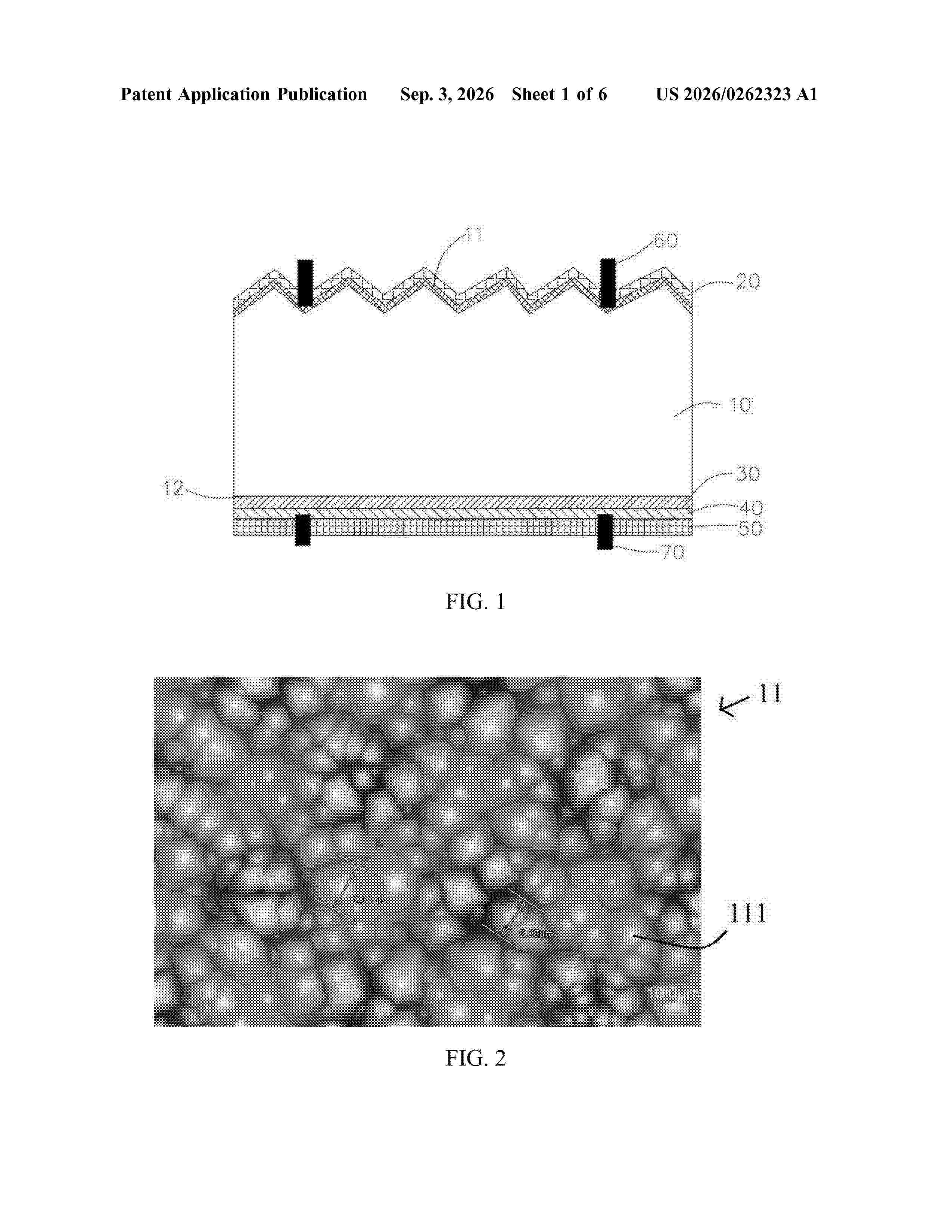
Resumen de: US20260262323A1
A solar cell includes a semiconductor substrate, in which a rear surface of the semiconductor substrate having non-pyramid-shaped microstructures, the non-pyramid-shaped microstructures include two or more first substructures at least partially stacked on one another, and a one-dimensional size of the surface of the outermost first substructure is less than or equal to 45 μm; a first passivation layer located on a front surface of the semiconductor substrate; first and second tunnel oxide layers located on the non-pyramid-shaped microstructures; first and second doped conductive layers located on a surface of the first and second tunnel oxide layers, the first and second doped conductive layer has different conductive types; a second passivation layer located on a surface of the first and second doped conductive layers; and electrodes formed by penetrating through the second passivation layer to be in contact with the first and second doped conductive layers.
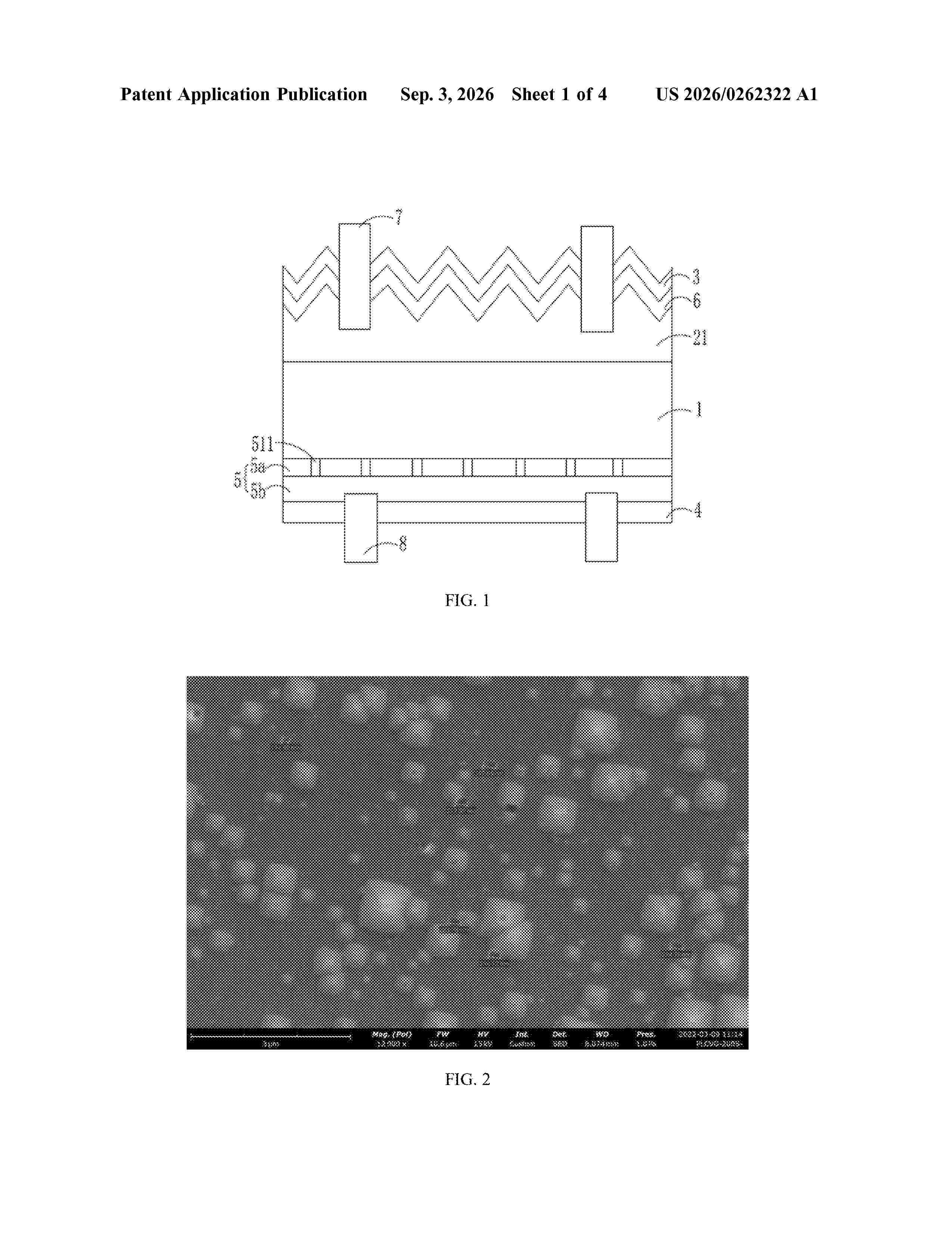
Resumen de: US20260262322A1
0000 In one aspect, a passivated contact structure includes a passivation oxide layer arranged close to a silicon wafer of a solar cell and a doped crystalline silicon layer away from the silicon wafer, wherein the thickness of the passivated oxide layer is 1.5 nm to 3.5 nm, and several nanoscale micropores are distributed in the passivated oxide layer.
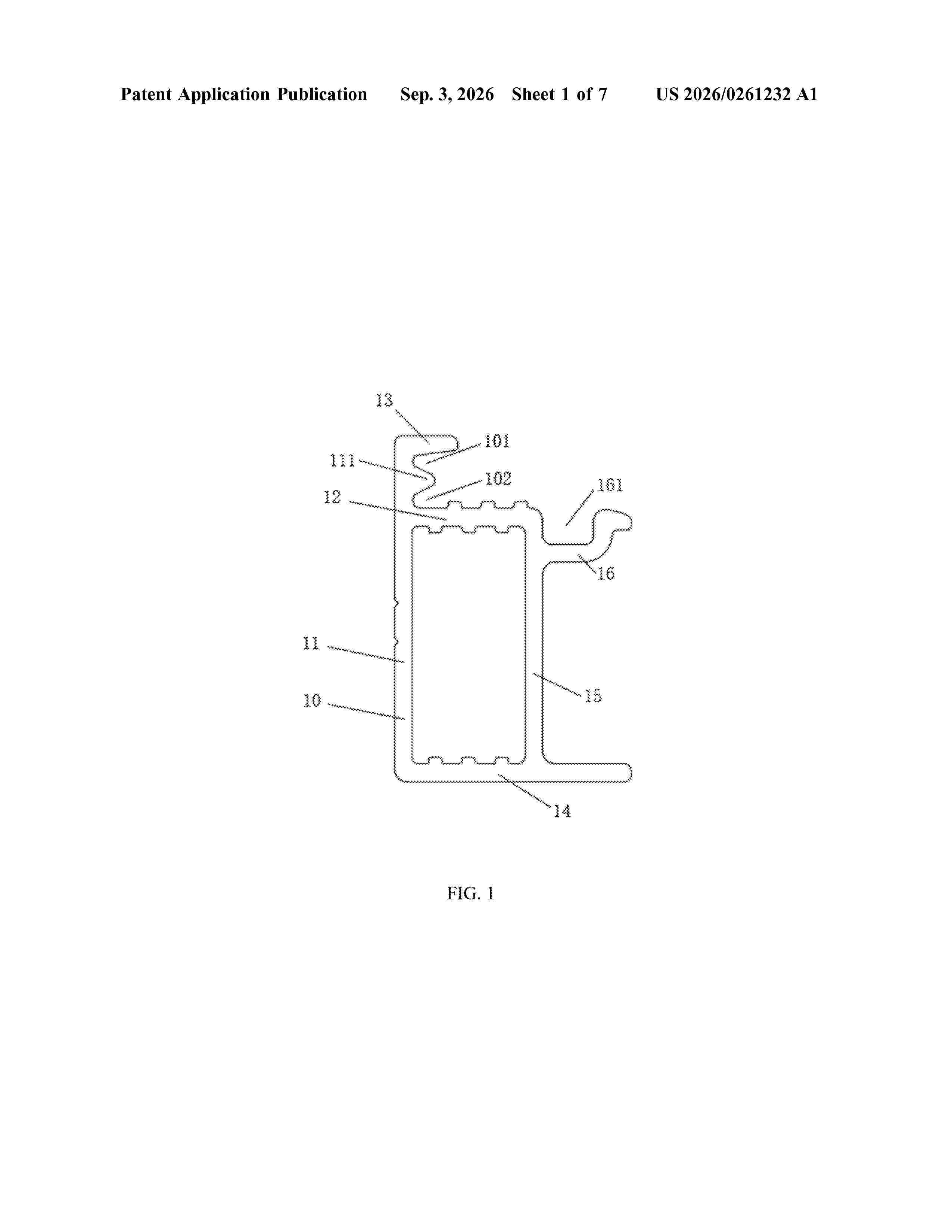
Resumen de: US20260261232A1
This application discloses a photovoltaic module and frame and a photovoltaic module. In one example, a photovoltaic module frame includes: a side plate, a bottom plate and a baffle plate that are fixed to a first side of the side plate. When the bottom plate is bonded to the bottom surface of the photovoltaic laminate, a surface of the baffle plate facing away from the bottom plate is lower than or flush with a light receiving surface of the photovoltaic laminate. The bottom plate, the side plate, and the baffle plate enclose a groove. A first protruding structure extending along a length direction of the side plate is arranged on the side plate. The groove is divided by the first protruding structure into a first overflow groove and a second overflow groove.
Nº publicación: US20260261229A1 03/09/2026
Solicitante:
ENSTALL US INC [US]
Enstall US, Inc.
Resumen de: US20260261229A1
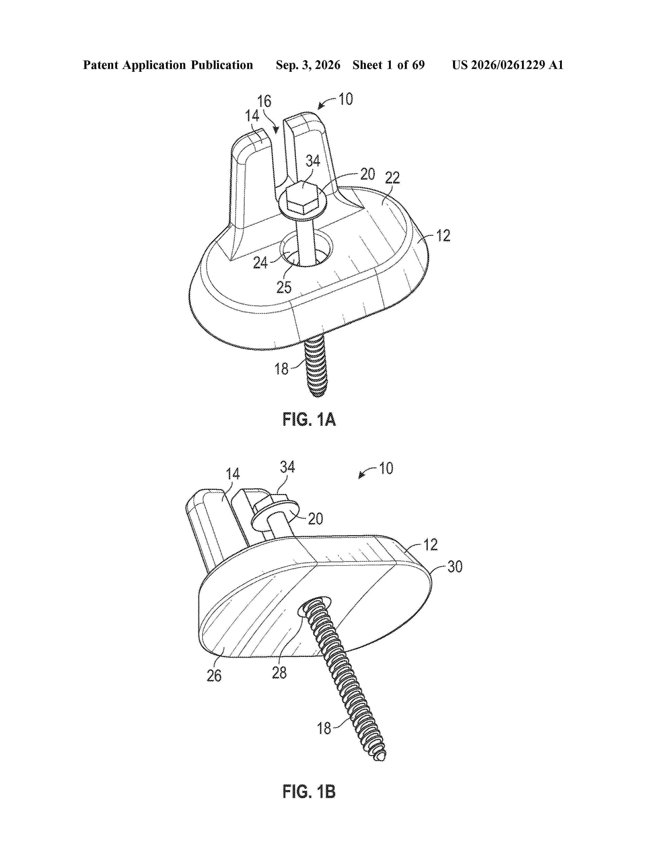
A mount assembly for securing a solar panel rail or rail-less support structure directly to a roof surface, the mount assembly including: a base having a top surface and a bottom surface; a guide extending upwards from the top surface of the base, where the guide forms a pair of members extending from opposing sides of the base and an aperture between the pair of members; a cavity formed within the base, where the cavity has an open end and a bottom cavity surface, where the open end is open relative to the top surface of the base; a through-hole, where the through-hole passes from the bottom cavity surface to the bottom surface of the base; a fastener, where the fastener is sized to pass through the through-hole; and a piston member, where the piston member is configured to surround a portion of the fastener.
 BOPI
BOPI
 Sede Electrónica