Si deseas distinguir tus productos, servicios o ambos de los de otra empresa, es posible que necesites una marca o nombre comercial. Descubre qué son, en qué consiste su procedimiento de registro y qué implica.

Información sobre los plazos de presentación de solicitudes de transformación de marcas de la Unión Europea en marca nacional española. Más información


Si tienes un nuevo dispositivo, producto o procedimiento que resuelva un problema técnico o tenga una ventaja práctica, existen distintas formas de protegerlo en España y en otros países. Descubre cómo hacerlo.

¿Tu innovación reside en la estética, la ornamentación o la apariencia de tu producto? Protégela mediante un diseño industrial. Descubre qué derechos confiere el registro y cómo realizar la tramitación.

Las indicaciones geográficas protegen el nombre de un producto originario de una zona geográfica, a la cual le debe una determinada calidad, reputación u otra característica. Descubre qué son, en qué consiste su procedimiento de registro y qué beneficios conceden.

Las patentes publicadas en todo el mundo son una valiosa fuente de información científica, técnica y comercial.

Si eres emprendedor/a o una empresa y quieres potenciar y mejorar la rentabilidad de tu negocio protegiendo de forma adecuada los activos intangibles de tu organización, en este espacio encontrarás lo necesario.


 161
resultados
161
resultados
 Última actualización
15/09/2026 [08:03:00]
Última actualización
15/09/2026 [08:03:00]


 Resultados 50 a 75 de 161

Resumen de: US20260269778A1
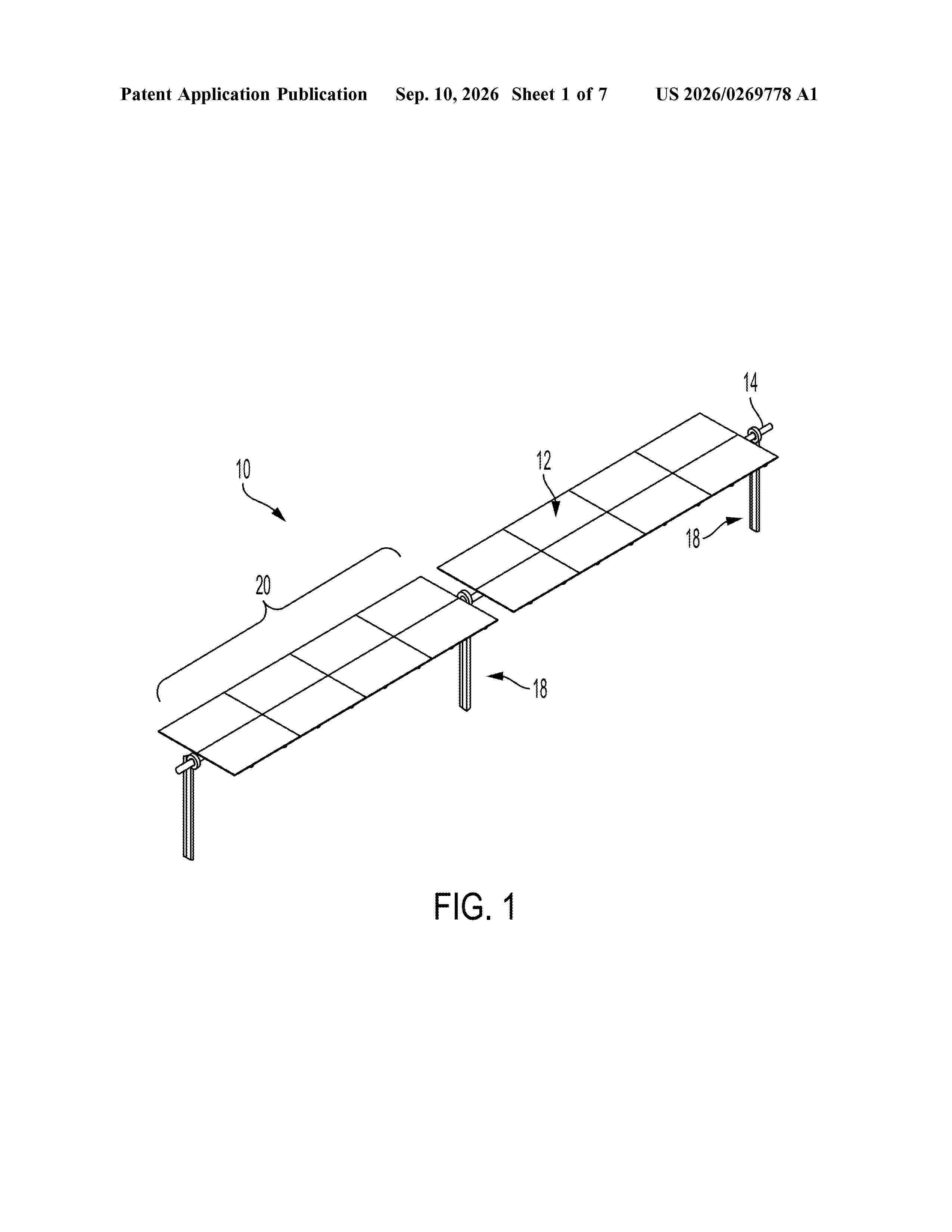
A tandem vehicular photovoltaic maintenance system includes a first vehicle, a second vehicle, a maintenance assembly, and a controller. The first vehicle includes a first vehicle body and one or more wheels coupled to the first vehicle body. The second vehicle includes a second vehicle body and one or more wheels coupled to the second vehicle body. The maintenance assembly includes a brush, and the maintenance assembly is supported at the first vehicle body and at the second vehicle body. The controller is coupled to the maintenance assembly, and the controller is configured to adjust a positioning of the brush relative to each of the first vehicle and the second vehicle and to cause the brush to be rotatably driven relative to each of the first vehicle and the second vehicle.

Resumen de: US20260269783A1
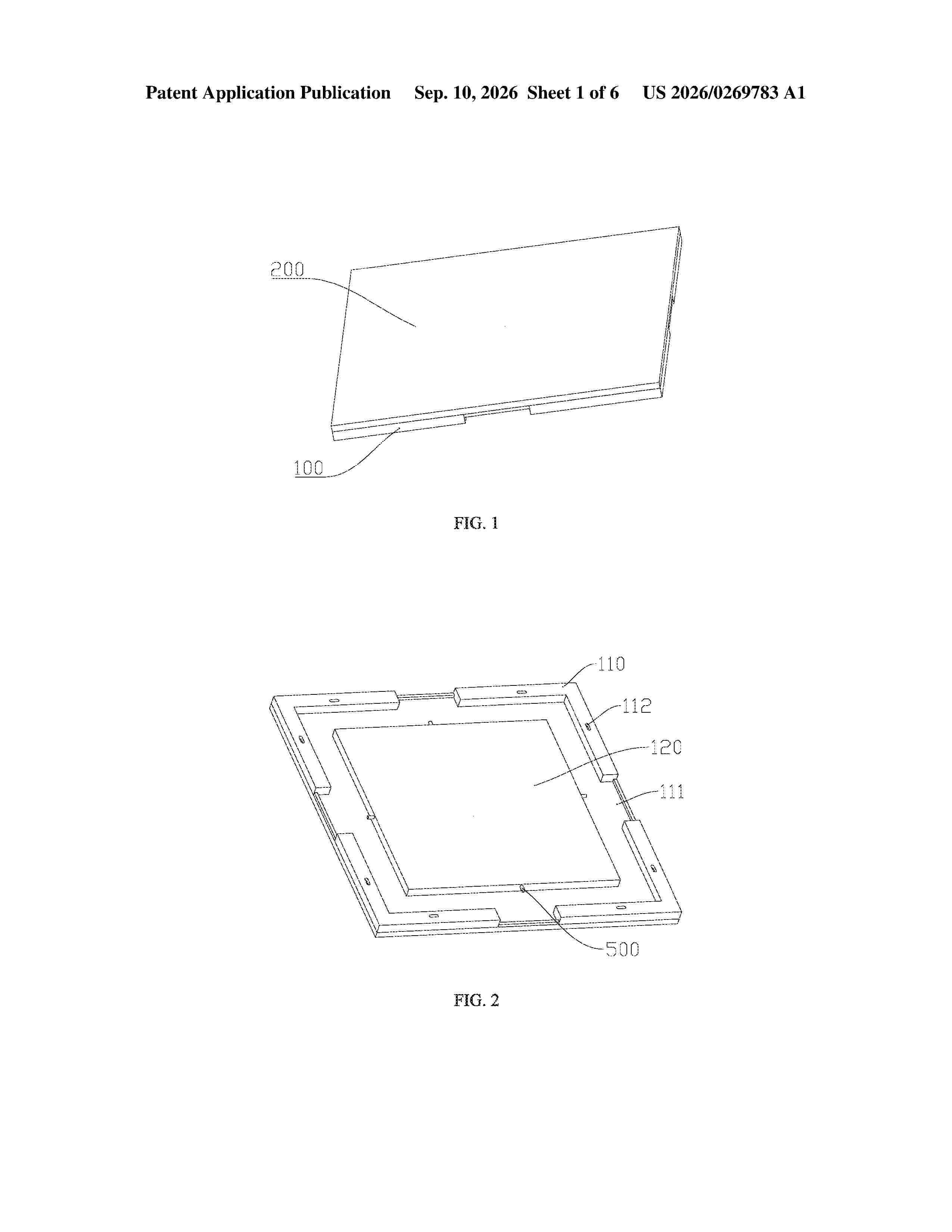
0000 Provided is a solar energy power supply integrated module unit,. The unit mainly includes: a housing component; a solar panel provided on the housing component, and a light facing surface of the solar panel is exposed from the housing component, a main control module provided inside the housing component and electrically connected to the solar panel; an energy storage battery provided inside the housing component and electrically connected to the main control module; an expansion or load interface, electrically connected to the main control module and/or the energy storage battery, and connected to a load or an expansion or load interface of another integrated solar energy supply and storage module unit; and a shell splicing module configured to connect a housing component of another solar energy power supply integrated module unit.
Resumen de: US20260266338A1
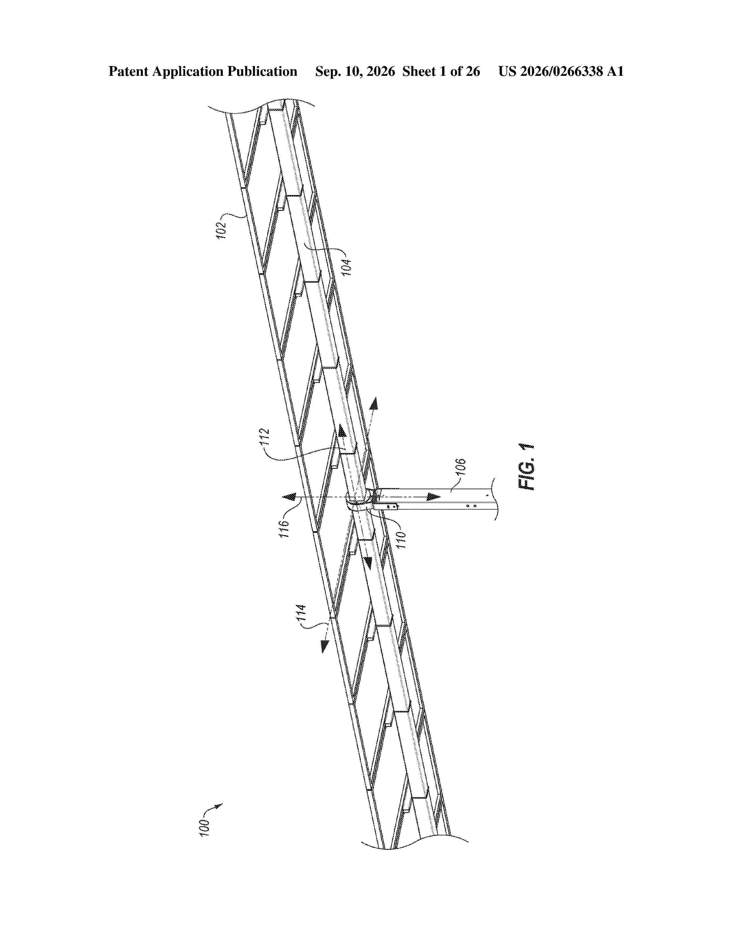
A variable angle torque tube interface is provided that includes a bearing configured to be coupled to a torque tube. The bearing may have an external surface that includes a rounded portion and a portion that defines a circumferential channel. The variable angle torque tube interface may also include a bearing housing coupled to the bearing that defines an axial channel and has a rounded internal surface portion. The variable angle torque tube interface may also include a pin positioned at least partially within the circumferential channel and at least partially within the axial channel to allow the at least some rotation by the bearing within the bearing housing about a tracking axis, a pitch axis, and a yaw axis and limit an amount rotation by the bearing within the bearing housing about the tracking axis.
Resumen de: US20260266462A1
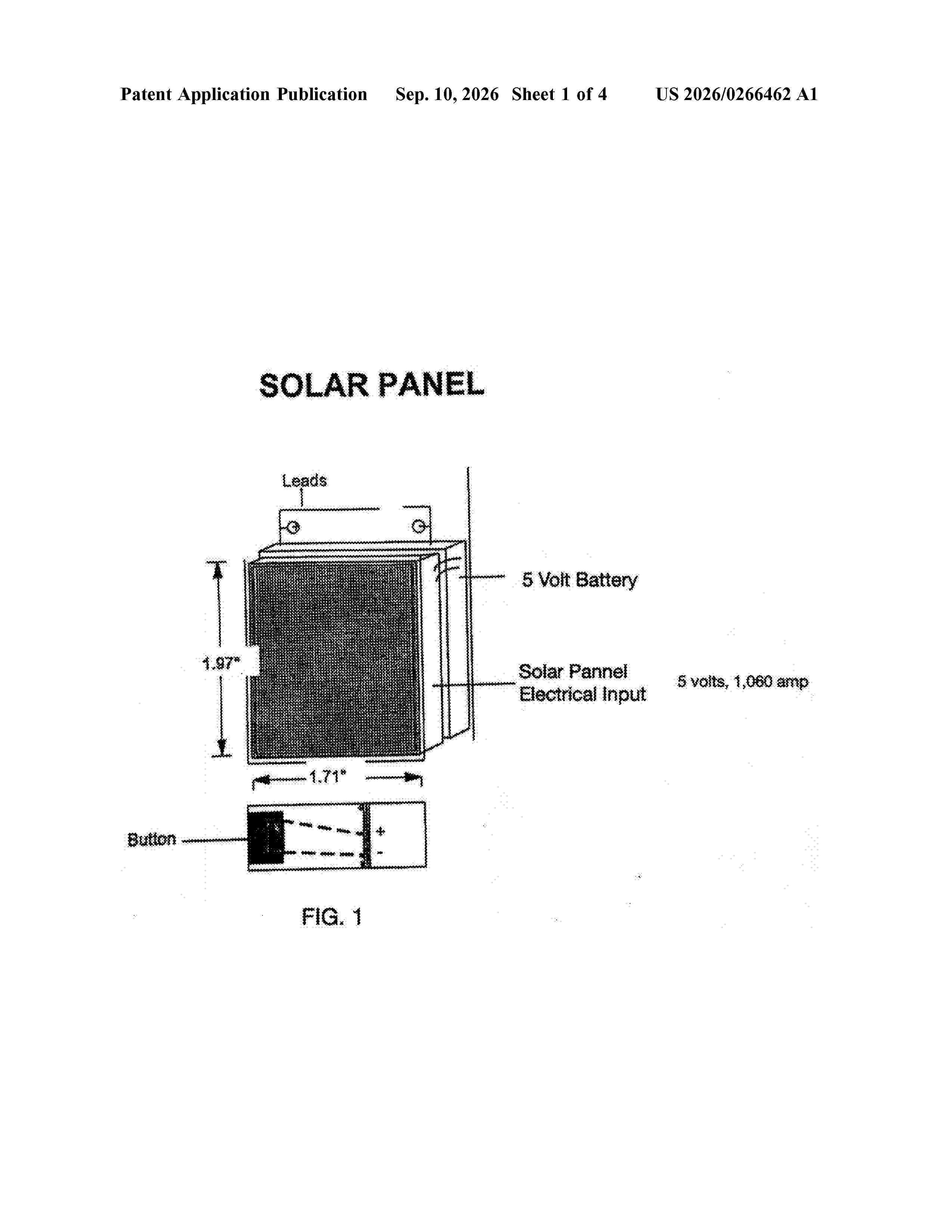
The invention comprises of solar cell(panel), along with a rechargeable lithium-ion battery, electronic circuit which is connected with the battery and the glow coil, so that, it can be recharged with a DC, or AC, household outlet.And the main purpose of the invention is intended to lit up cigarettes for smokers, with it's glow coil.
Resumen de: US20260269777A1
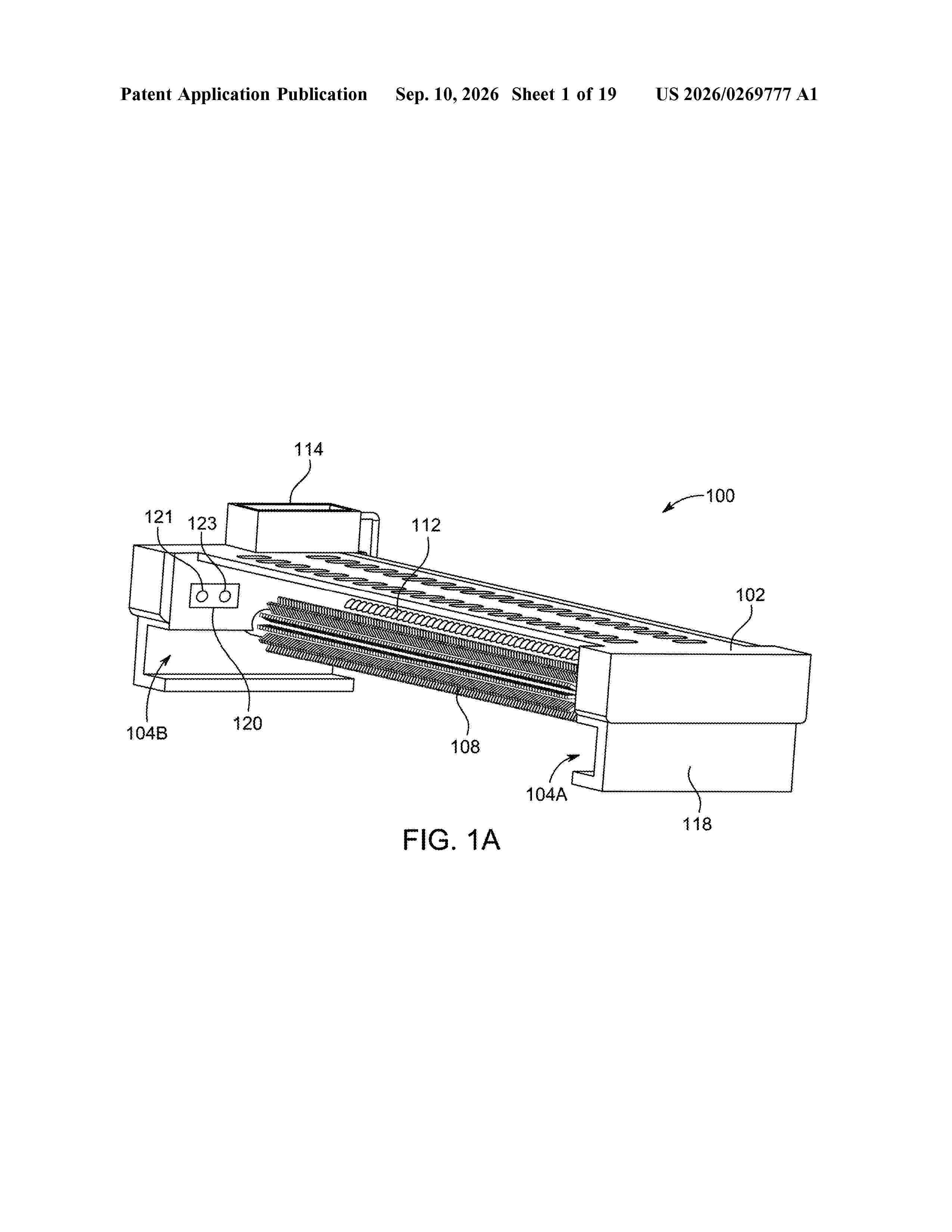
A solar panel system includes solar panels and a frame that has slider structures on two sides and is configured to receive the solar panels. A brush cleaner, including two end structures coupled with the slider structures, slides along the frame to clean the solar panels. The brush cleaner includes a brush extending between the end structures and a plate with air nozzles configured to blow air based on dust detection. The solar panel system further includes a light source emitting source light towards the solar panels, an optical sensor detecting dust based on received light, and an air compressor box positioned on one end of the plate. The air compressor box is mounted on one end structure of the brush cleaner such that the air compressor box does not obstruct the source light, received light, or airflow from the nozzles.
Resumen de: WO2026185907A1
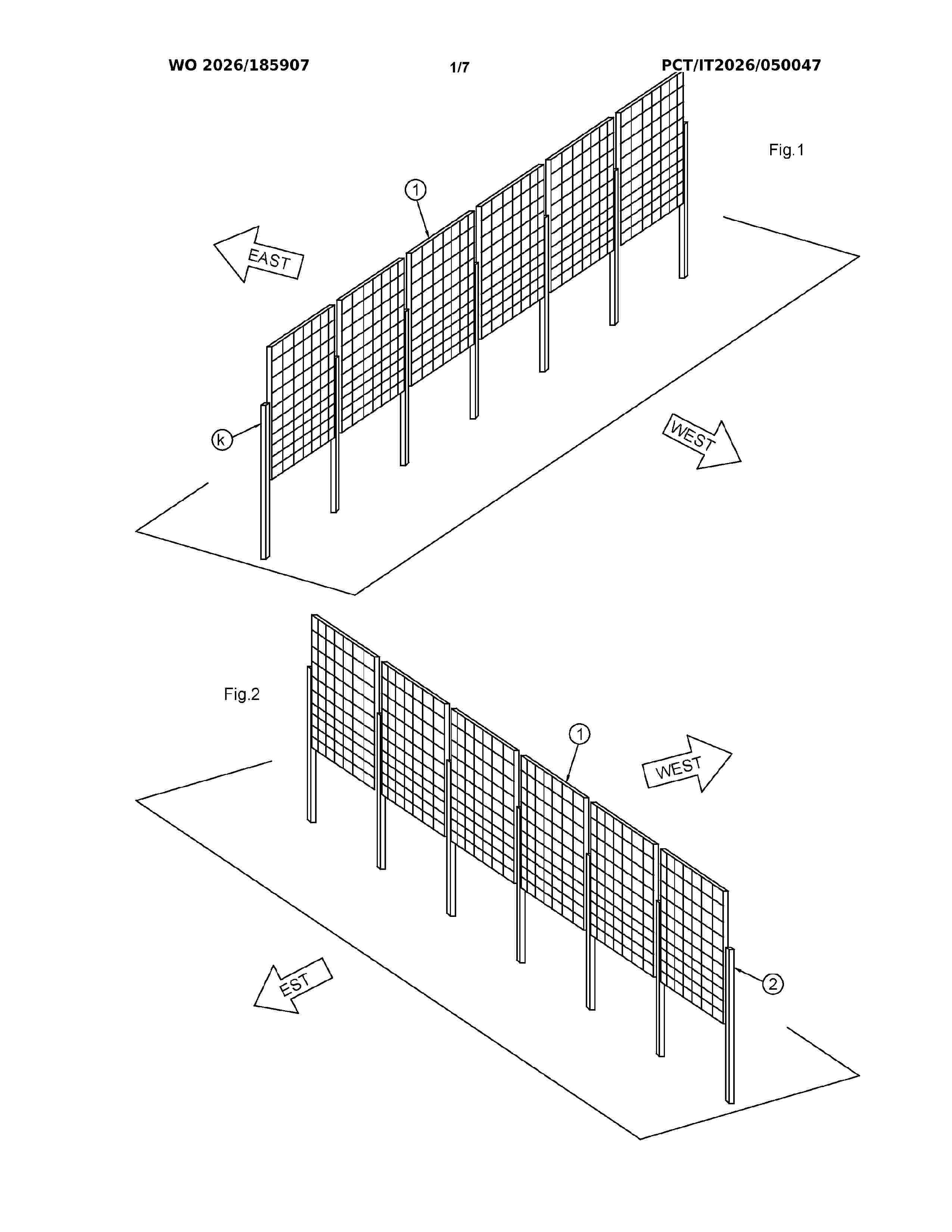
Field of bifacial photovoltaic solar panels (1 ) comprising bifacial photovoltaic panels arranged in rows in a NORTH-SOUTH direction, each of said bifacial photovoltaic panels being equipped with two solar radiation collection surfaces, each row of bifacial photovoltaic panels also comprising poles (K) fixed into the ground and panels arranged between one pole and another, each bifacial photovoltaic panel being constrained on one side to a pole (K) and on the other side to the next pole (K) with lateral constraints that allow rotation, in which the axis passing through the lateral constraints is arranged at a certain distance above the axis passing through the centre of gravity of the panel, characterised in that each panel (1 ) on one side is rotatably constrained to a pole while on the other side the panel is rotatably constrained to an intermediate point (4) of a crank (5) which at one end (2R) is rotatably constrained to said other pole and which at the opposite end (5A) is connected to one end of a linear actuator (7) which is in turn connected to the opposite end to the panel (1 ) to be able to modify its inclination, so that the rotating constraint (2L) of the panel (1 ) with the pole (K) has a different height from the rotating constraint (4) of the panel (1 ) with the crank (5).
Resumen de: WO2026185585A1
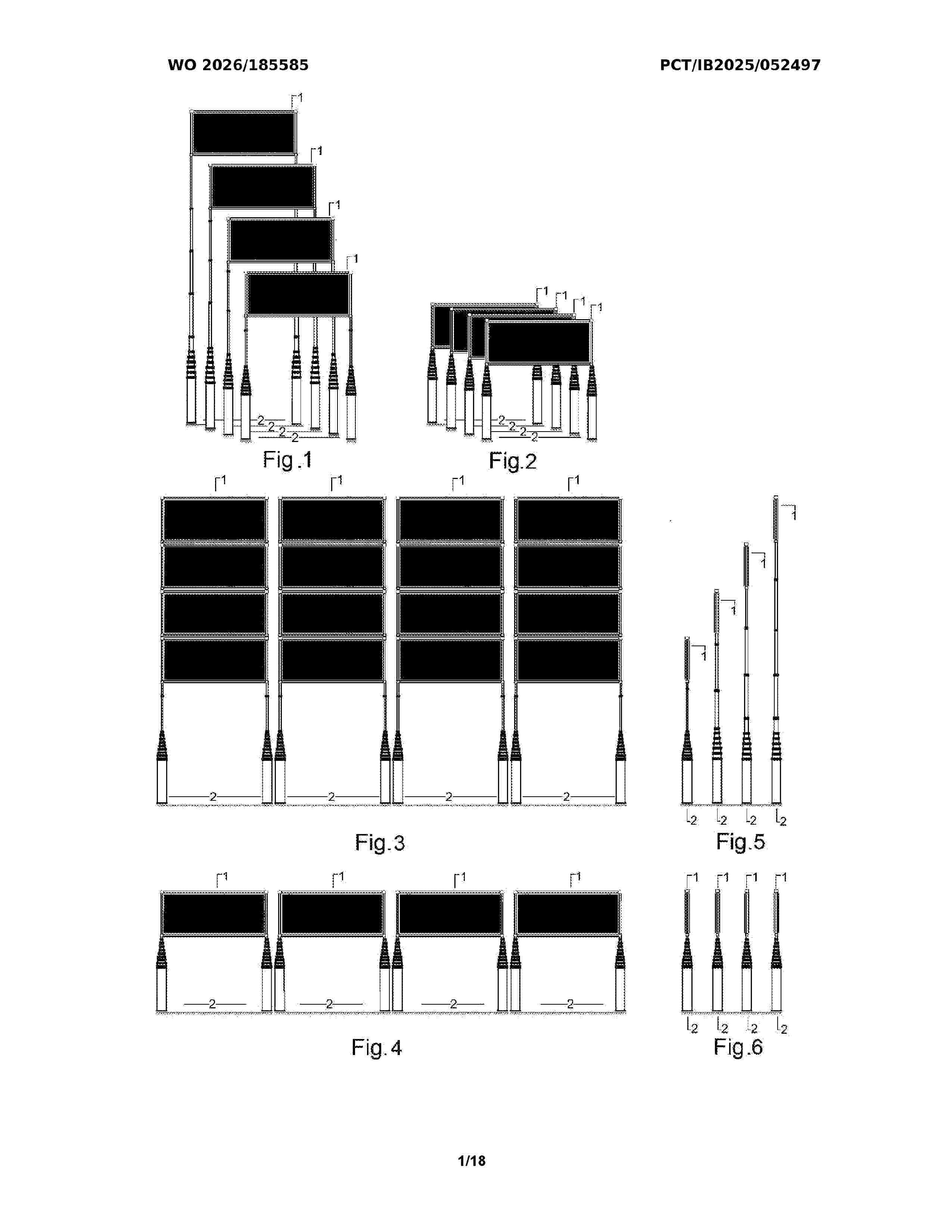
Mobile Photovoltaic Station (1) located on marine and/or wheeled mobile platforms (8), with possibility to use on a ground location. The station is equipped with multi-level shadowless photovoltaic terraces (2), mounted on support mechanisms (3) allowing their extension from a StandBy position to a full extended working position. For optimal positioning of the station to solar radiation, a solar radiation meter is used. On watercraft, an anchor midship system (14) together with thrusters and a propeller to align the vessel. On land or on a truck, a two-level support platform (56) connected by a rotating mechanism is used. Solar radiation positioning systems are controlled automatically, or manually, on the mobile platforms themselves or by an onshore operator for offshore platforms via a cable-buoy connection. The Mobile Photovoltaic Station uses electricity from the station's battery system for propulsion and can recharge on the move or use a hybrid electrical generator.
Resumen de: WO2026185715A1
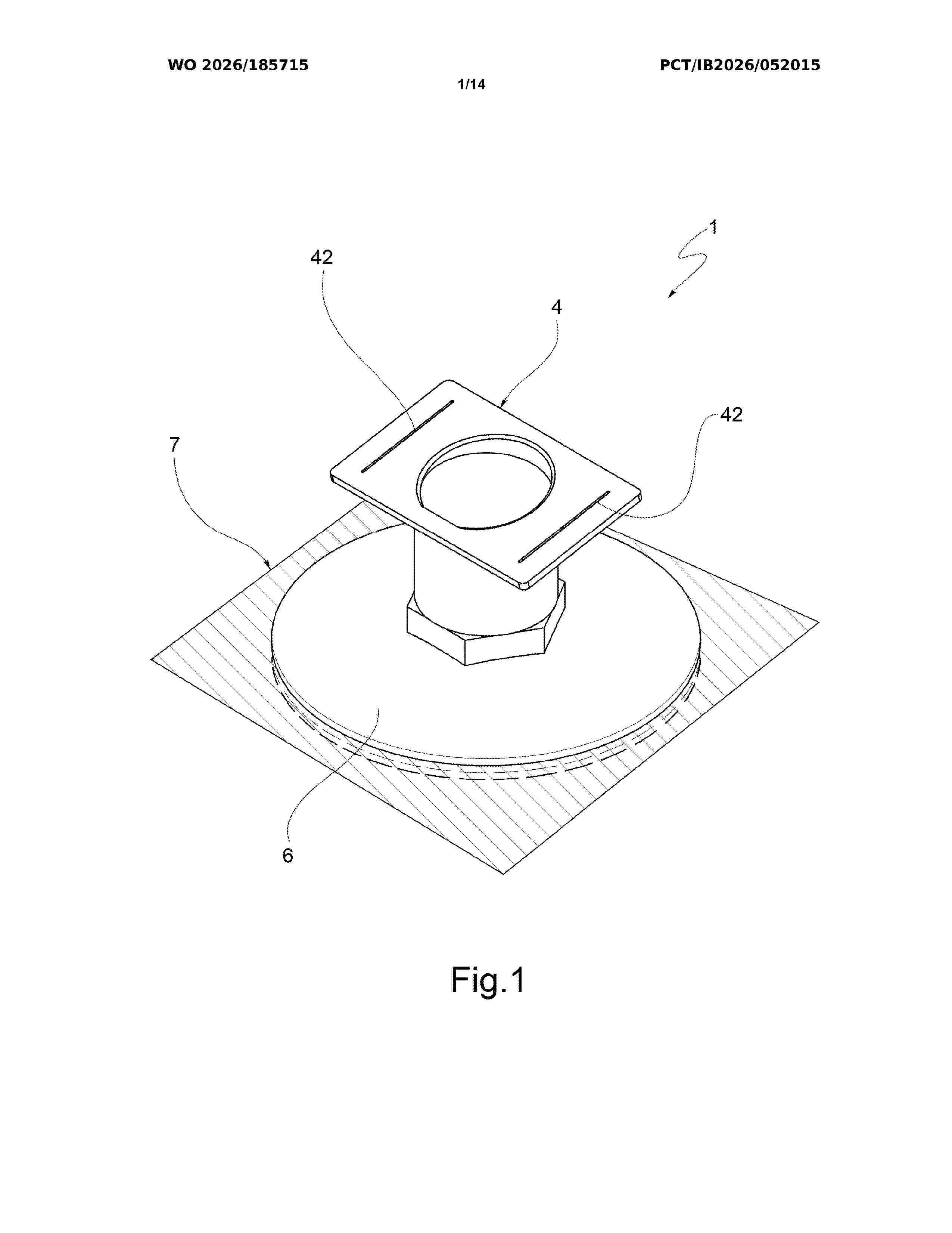
The present invention relates to a support device (1; 10) suitable for being applied to a roof (2). Such support device comprises an anchoring element (3) and a support element (4). The anchoring element (3) is suitable for being applied to the roof (2) by mechanical connection and/or shape coupling and/or force coupling. Further, such anchoring element (3) comprises an anchoring base (30) engageable with the roof (2) and a substantially cylindrical coupling body (31) projecting from the anchoring base (30) along a device extension axis (V). The support element (4) is configured as a support for applying a guide or installation (9) to be mounted on the roof (2). Such support element (4) comprises a support platform (40) on which the guide or the installation (9) is installable, and a substantially cylindrical connection body (41) projecting from the support platform (40). The coupling body (31) and the connection body (41) mutually engage by mechanical connection and/or shape coupling and/or force coupling.
Resumen de: WO2026185046A1
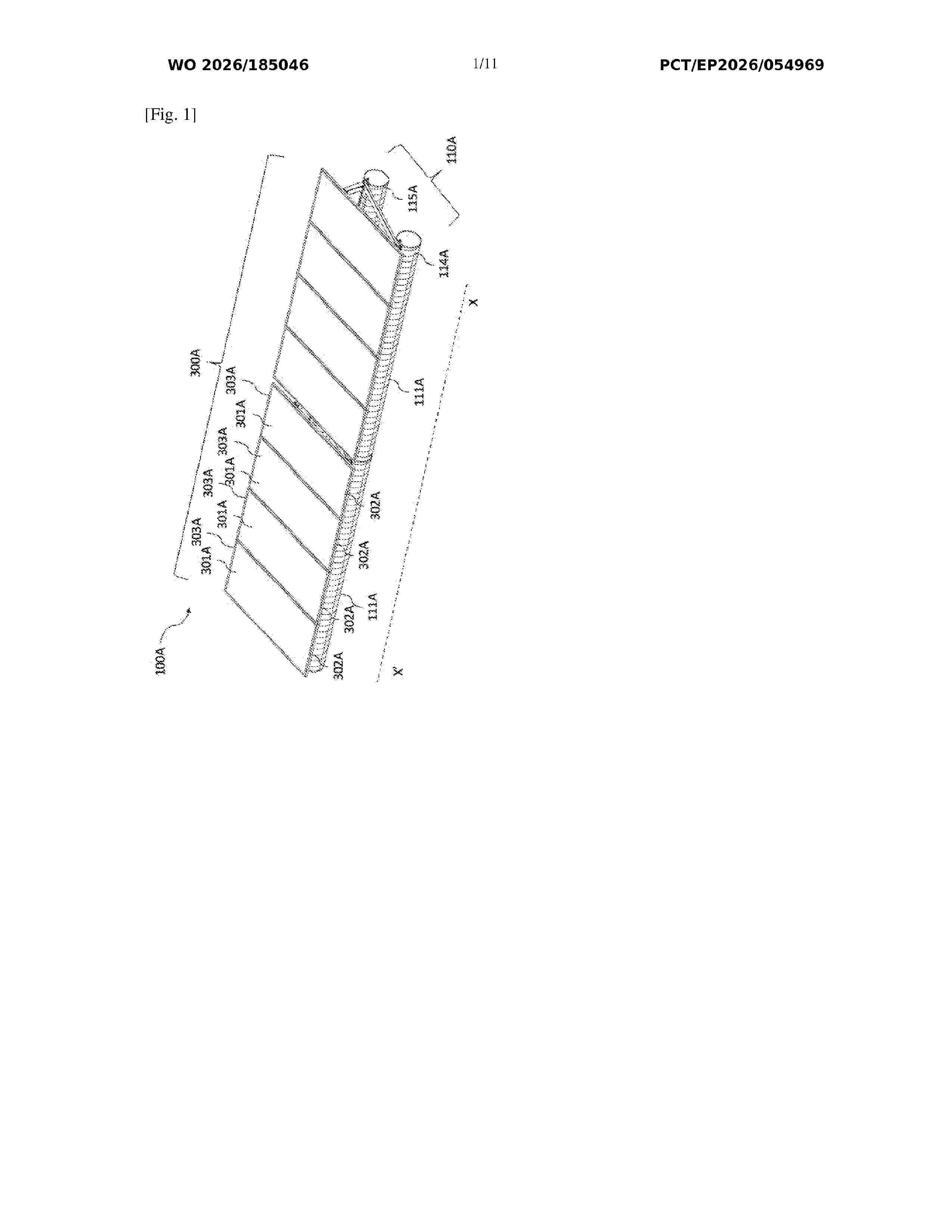
The invention relates to a floating photovoltaic system comprising: - a pair of rows of hollow cylindrical floats, each float (111A) comprising a plurality of attachment supports arranged and aligned on an outer surface; - a series of photovoltaic panels 300A, each panel of the series being attached, via at least one of its sides, to two of the attachment supports of two floats (111A) of one and the other of the two rows of a pair of rows among the at least one pair of rows of floats; the photovoltaic system being characterised in that a profiled portion is arranged, via one of its faces referred to as the contact face, against an inner surface of each float (111A) and such that the attachment supports of each float (111A) are aligned in the elongation direction and mechanically connected to the profiled portion.
Resumen de: WO2026187227A1
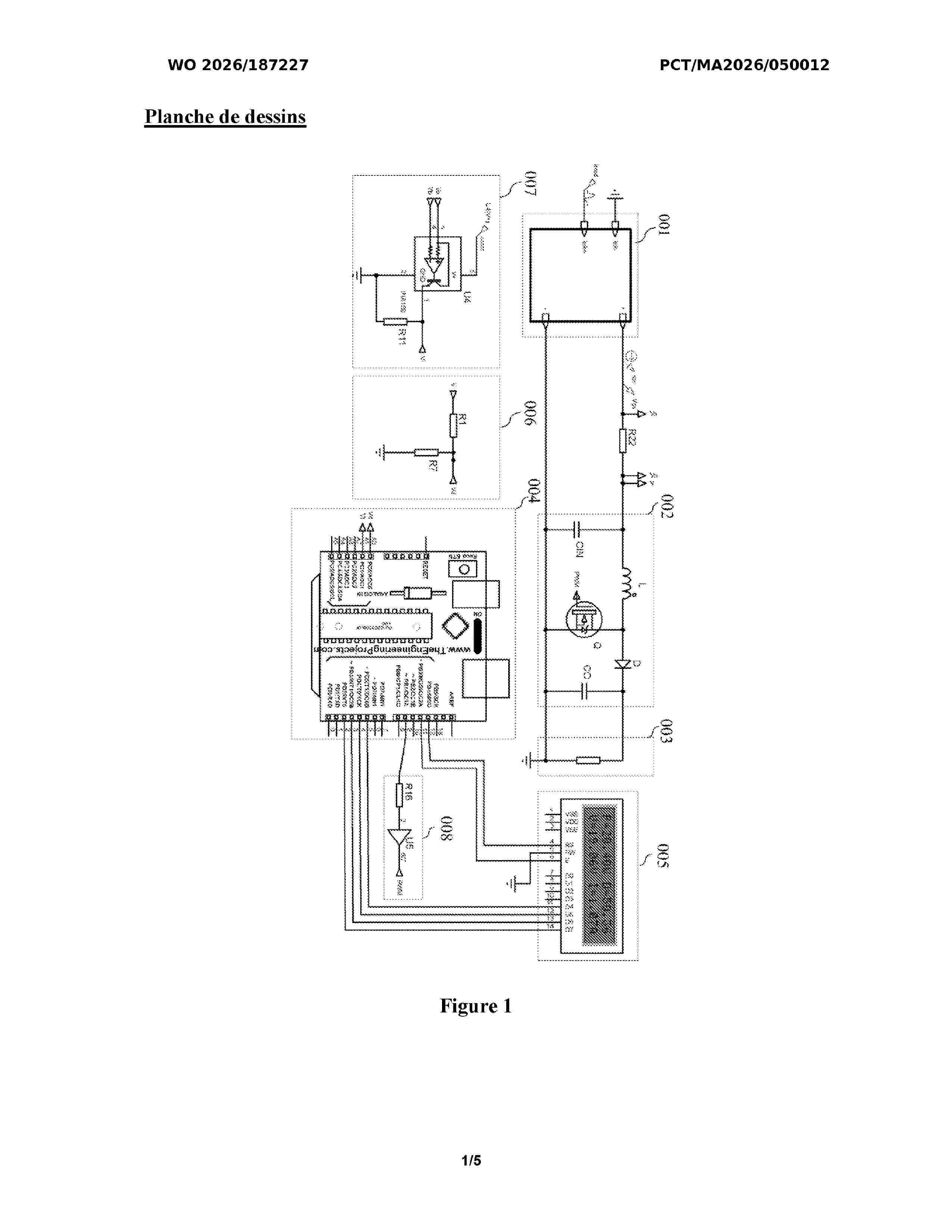
: The present invention proposes an innovative maximum power point (MPP) tracking device that is optimized for photovoltaic (PV) systems. Based on an improved perturb-and-observe (P&O) algorithm and integrated proportional-integral (PI) control, this device integrates a maximum power point tracking (MPPT) method with a mechanism having an adaptive step size. Replacing the traditional voltage perturbation with a current perturbation considerably improves tracking accuracy and efficiency, thus reducing energy losses. The assembly is implemented at low cost on an Arduino Uno microcontroller using a C++ code that is optimized to integrate the PI control directly, eliminating the need for external components. This solution offers enhanced performance, a simplified architecture and reduced costs, outperforming not just conventional methods but also advanced techniques such as particle swarm optimization (PSO) and fuzzy logic control (FLC).
Resumen de: WO2026185675A1
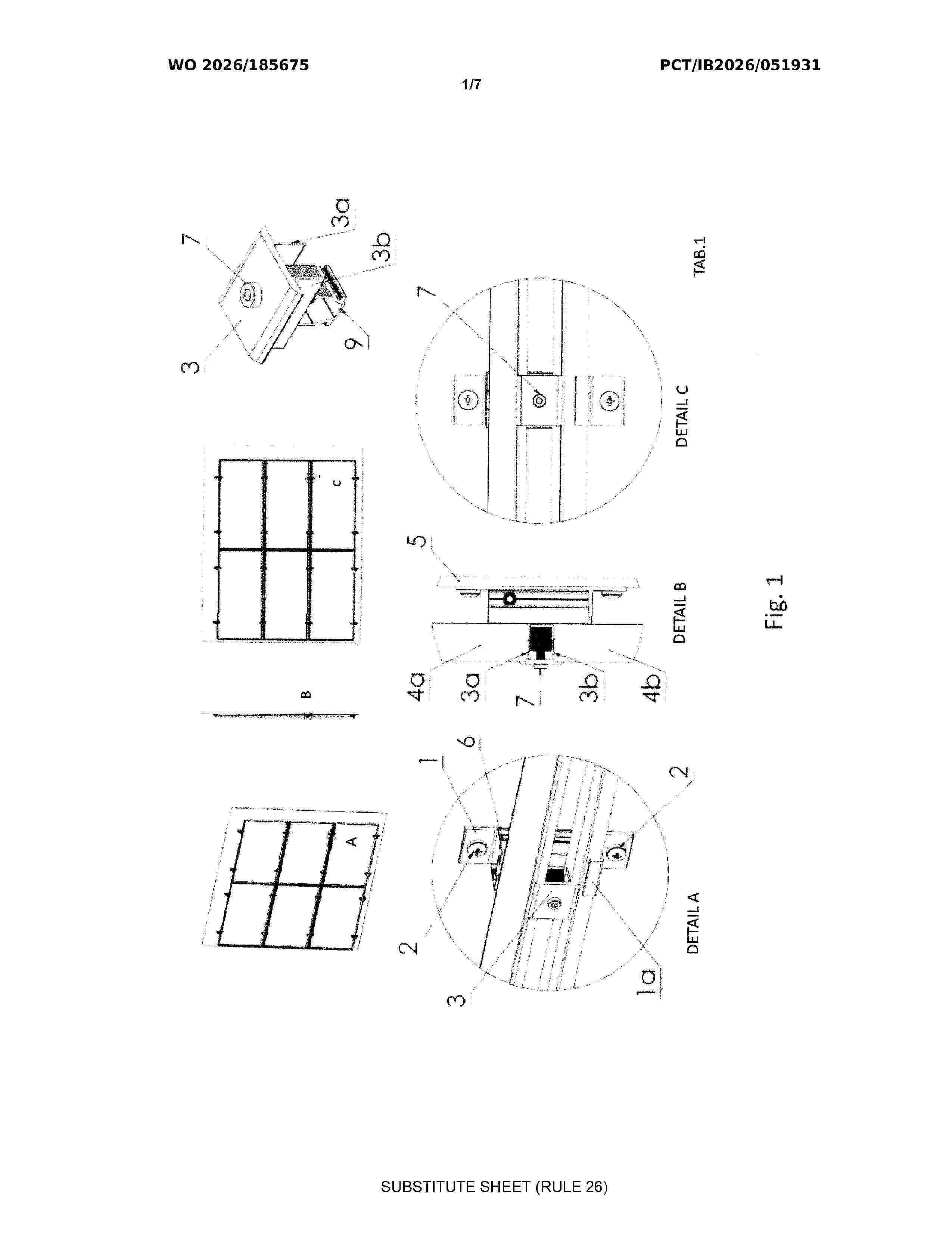
Mounting system for vertical photovoltaic facades or walls, configured for the vertical mounting of at least one photovoltaic module, comprising a main support kit comprising : an upper load-bearing profile (6) having a substantially U-shaped section and provided with at least two winged surfaces (6a, 6b); a lower load-bearing profile (1) provided with two base wings (1f, 1g) each comprising over a surface a pass- through eyelet (1b, 1c), and a vertical surface (1i); said upper load-bearing profile (6) and said lower load- bearing profile (1) being able to be mutually connected and fixed by means of fastening means. Said lower profile (1) comprises a substantially cylindrical groove (1d) into which is able to be inserted a screw (8) configured to fix the lower load-bearing profile (1) to the upper load-bearing profile (6).
Resumen de: WO2026185669A1
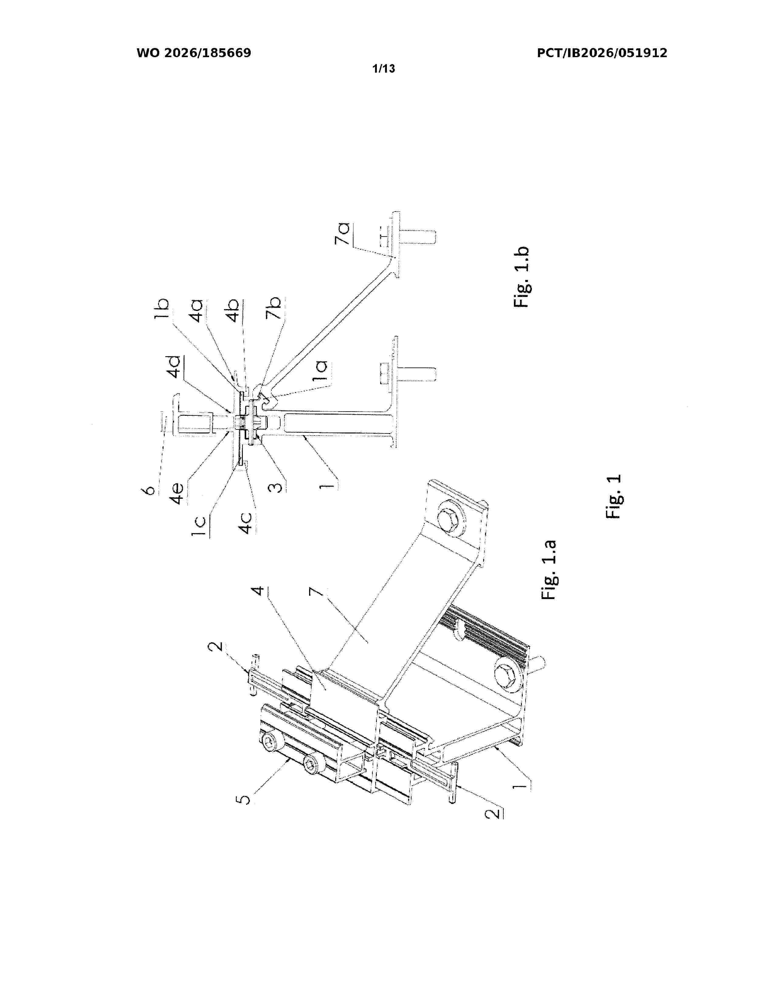
Mounting system for vertical photovoltaic facades or walls, comprising a load-bearing support (1) provided with: - at least one base wing (1l) for fixing to a wall, - a groove (1d), - a plurality of slotted holes (1f, 1g), and - modular accessories for mounting photovoltaic modules in both vertical and horizontal orientation, said accessories being selected from the group consisting of: - a terminal fixing kit - a central fixing kit.
Resumen de: DE102025108948A1
Die Erfindung betrifft ein Bautenschutzelement (10; 100; 300) mit zumindest einer ersten nutartigen Ausnehmung (12, 16) zur Aufnahme eines Tragelementabschnitts (214; 414) eines ein Solarmodul (210) tragenden Tragelements (212; 412), sowie mit Lastaufnahmeflächen (20, 22, 24, 26) zur Abstützung von Montagegewichten (216; 416). Die Erfindung betrifft zudem eine Solarmodulanordnung.
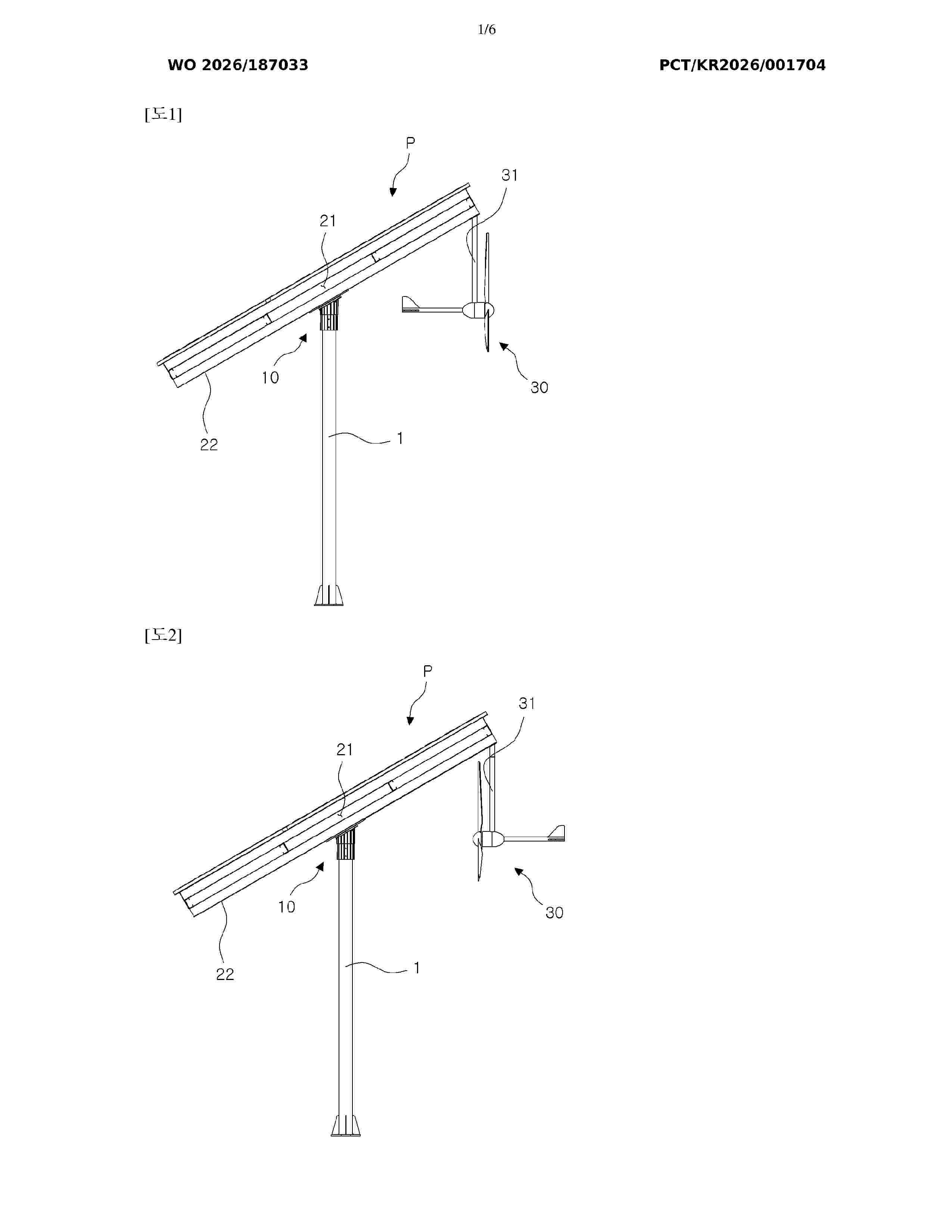
Resumen de: WO2026187033A1
Disclosed is a convergence power generation system comprising: a solar panel array; a wind power generator that is disposed around the solar panel array and movable in conjunction with rotation of the solar panel array; and a solar tracker that provides rotational force to the solar panel array.
Resumen de: DE102025000800A1
1. Schwimmende Flüssigbatterie, deren Elektrolytflüssigkeit aus Salzwasser bestehen kann.2. Bei Flüssigbatterien handelt es sich um eine Bauform von Energiespeichern, die elektrischen Strom in ihrem Speichermedium, welches in der Regel aus Salzwasser besteht, aufnehmen und wieder abgeben können. Stationäre Modelle mit kleiner Speicherleistung werden oft in Wohnhäusern installiert, in der Regel um Strom aus Photovoltaikanlagen, die direkt an der Immobilie verbaut sind, aufzunehmen, um diesen zeitversetzt wieder abgeben zu können. Es sind auch deutlich größere Anlagen bekannt, die im gewerblichen Bereich eingesetzt werden oder als Speicher für größere Wohnanlagen dienen. Ihre Verbreitung ist trotz vieler Vorteile auf Grund der höheren Entstehungskosten, die im Wesentlichen aus der geringen Speicherkapazität des verwendeten Salzwassers als Speichermedium resultieren, nicht besonders ausgeprägt.2.1 Um kostengünstige Flüssigbatterien bereitstellen zu können, wird eine schwimmende Flüssigbatterie, deren Elektrolytflüssigkeit (7) aus Salzwasser bestehen kann (1) Vorgeschlagen, die in einer reißfesten, wasserundurchlässigen Batteriehülle (3) untergebracht ist und in einem geeigneten, bestehenden oder dafür neu geschaffenen Gewässer (10) schwimmend so positioniert wird, dass der Innendruck in der wasserundurchlässigen Batteriehülle (3), der mehrheitlich durch die entsprechende Menge an Elektrolytflüssigkeit (7) erzeugt wird, von dem Außendruck des Gewässe
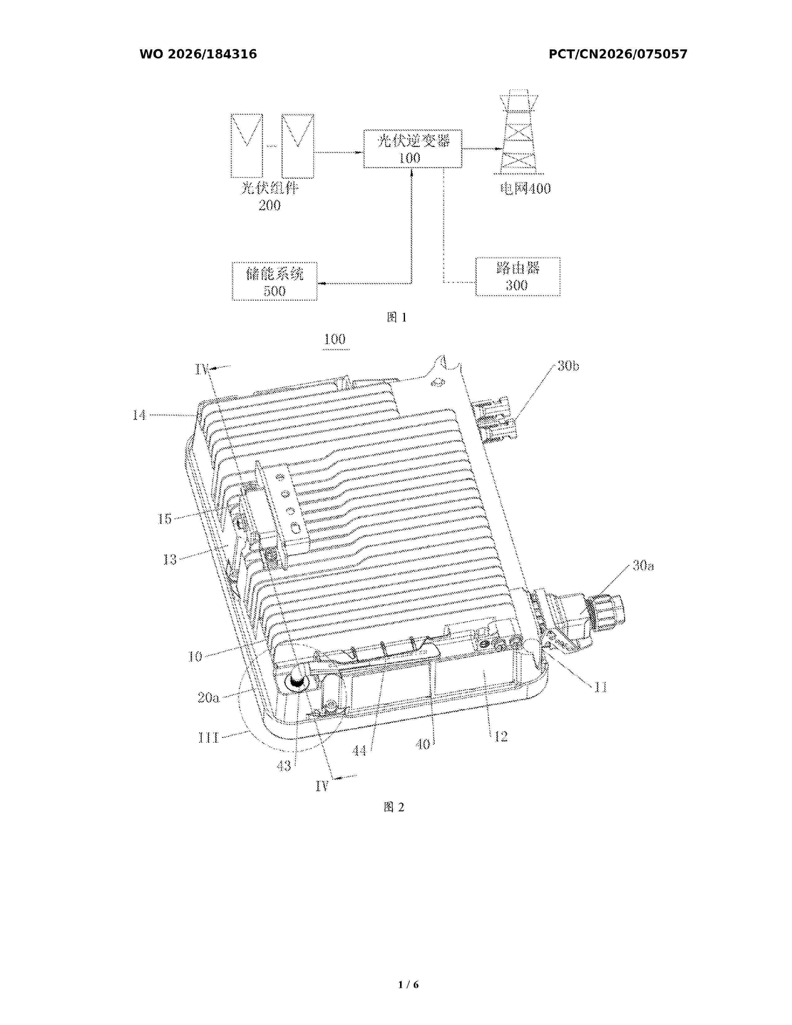
Resumen de: WO2026184316A1
A photovoltaic inverter (100), comprising a bottom housing (10), a top cover (20a), an alternating-current terminal (30a), a direct-current terminal (30b) and a communication antenna (40), wherein the bottom housing (10) and the top cover (20a) form an accommodating cavity (21); the bottom housing (10) comprises a first side face (11), a second side face (12), a third side face (13) and a fourth side face (14) which are connected in sequence, the first side face (11) and the third side face (13) being arranged opposite each other, and the second side face (12) and the fourth side face (14) being arranged opposite each other; the alternating-current terminal (30a) and the direct-current terminal (30b) are mounted on the first side face (11); the alternating-current terminal (30a) is configured for connecting to a power grid (400) or a load, and the direct-current terminal (30b) is configured for connecting to an energy storage battery or a photovoltaic module (200); the communication antenna (40) is mounted at the corner between the second side face (12) and the third side face (13); and the communication antenna (40) comprises a rotating structure (43) and a radiator (44), the rotating structure (43) is connected to the radiator (44), the rotating structure (43) is used for driving the radiator (44) to rotate in a plane perpendicular to the second side face (12) and the third side face (13), and the radiator (44) is used for transmitting or receiving electromagnetic waves. In
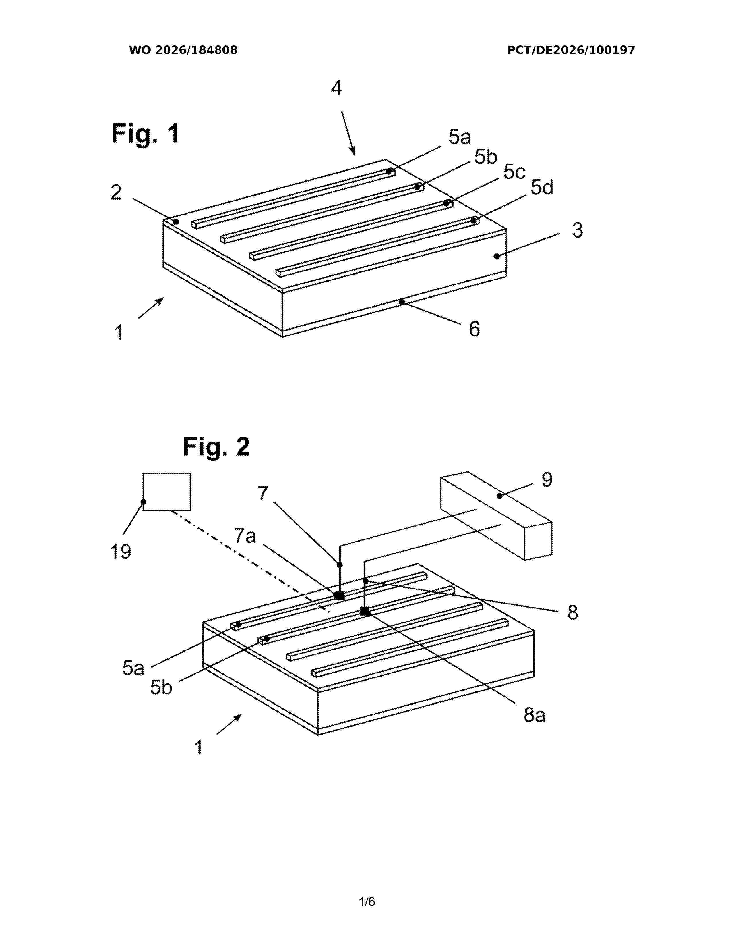
Resumen de: WO2026184808A1
The invention relates to a method for improving the ohmic contact behavior between a semiconductor wafer surface of a silicon wafer solar cell and a metal electrode structure which is applied to the semiconductor wafer surface and has multiple mutually separated metal contact fingers. The method is used on only one side of the silicon solar cell. A first contact finger (5a - 5d) is contacted by a first contacting means (7) electrically connected to a pole of a voltage source (9), and a second contact finger is contacted by a second contacting means (8) electrically connected to the other pole of the voltage source (9). When a voltage is generated by the voltage source (9), an electric field is applied between the first contact finger (5a - 5d) and the second contact finger (5a - 5d) along a portion of the semiconductor surface lying between the first and second contact fingers (5a - 5d), and when the electric field is applied, at least a solar-active subregion of the portion of the semiconductor surface lying between the first and second contact fingers (5a - 5d) is illuminated with a light source. A current flow generated by the electric field and the illumination in the portion of the semiconductor surface lying between the first and second contact fingers (5a - 5d) has a current density of 10 A/cm2 to 50,000 A/cm2, with respect to the area of the first contact finger (5a - 5d), and acts for a time of 10 ns to 3 s.
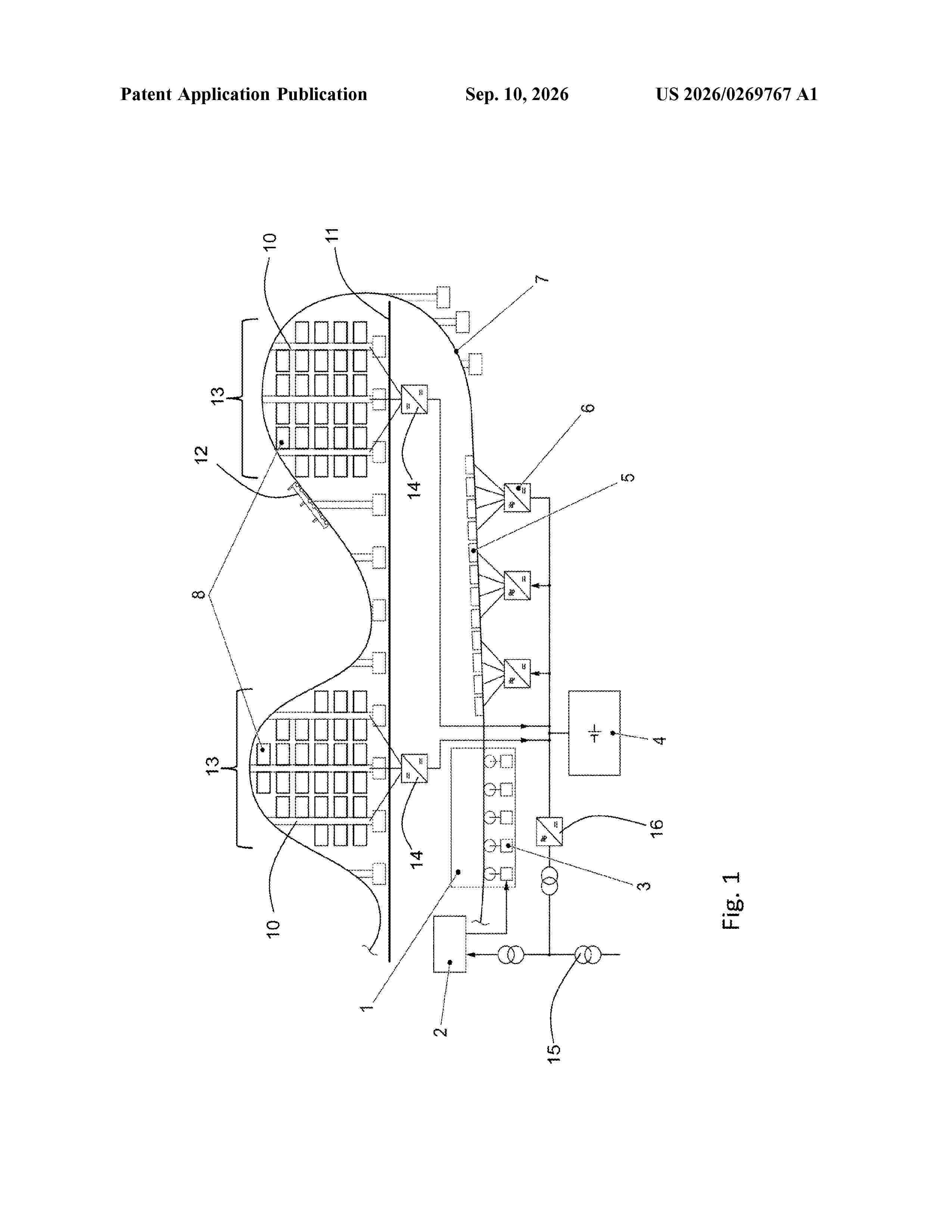
Resumen de: US20260269767A1
An amusement facility with a rail system and vehicles guided on the rail system includes a drive for powering the vehicles, as well as a power supply for the drive. The rail system includes elevated sections that are arranged vertically above a base area on a support structure, on which the amusement facility is built. A plurality of photovoltaic units and/or wind energy units for generating electrical energy are arranged on the supporting structure, which are connected to at least one energy storage system for storing the generated electrical energy. The at least one energy storage system is connected to supply electrical energy to the drive and/or a control unit for controlling the amusement facility.
Resumen de: EP4804767A1
0001 The present disclosure relates to the field of photovoltaic technology, and provides a segmented solar cell and a photovoltaic module, which is at least beneficial to improving the efficiency of the photovoltaic module. The segmented solar cell is formed by cutting a whole solar cell, and includes: a cell body having a first main surface, an opposing second main surface, and a first side surface and a second side surface connecting the first main surface and the second main surface, respectively; a first passivation stack formed on the first side surface, a second passivation stack formed on the second side surface, and a third metal oxide layer formed on a surface of the second passivation stack away from the cell body. The first side surface is a cut surface formed by cutting the whole solar cell, and the second side surface is an uncut side surface.
Resumen de: EP4804768A2
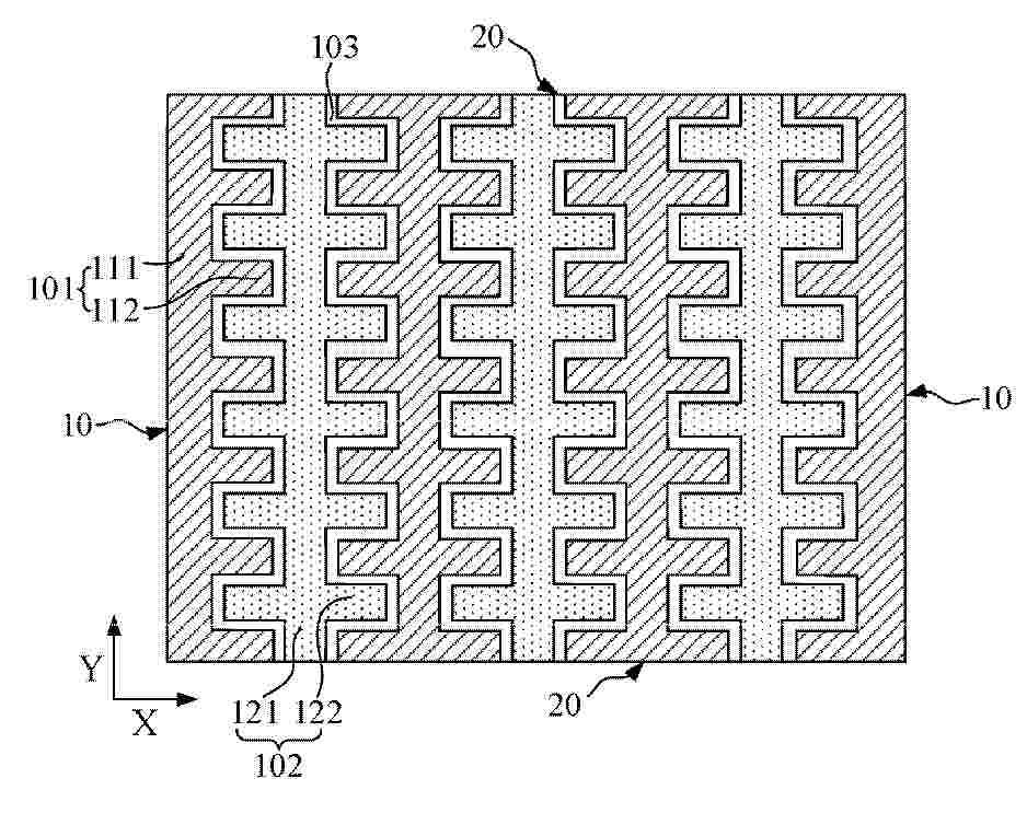
0001 Provided are a back-contact solar cell, a method for preparing the same, and a photovoltaic module. The solar cell includes a substrate, a plurality of first doped sections and a plurality of second doped sections. The substrate has a first side, and the first side has two opposing first edges perpendicular to a first direction and two opposing second edges perpendicular a second direction, the first direction being perpendicular to the second direction. The plurality of first doped sections are formed on the first side, and each first doped section includes a first portion extending along the second direction and a plurality of second portions distributed at intervals along the second direction, where each second portion protrudes from the first portion in a direction parallel to the second edges.
Resumen de: WO2025096397A1
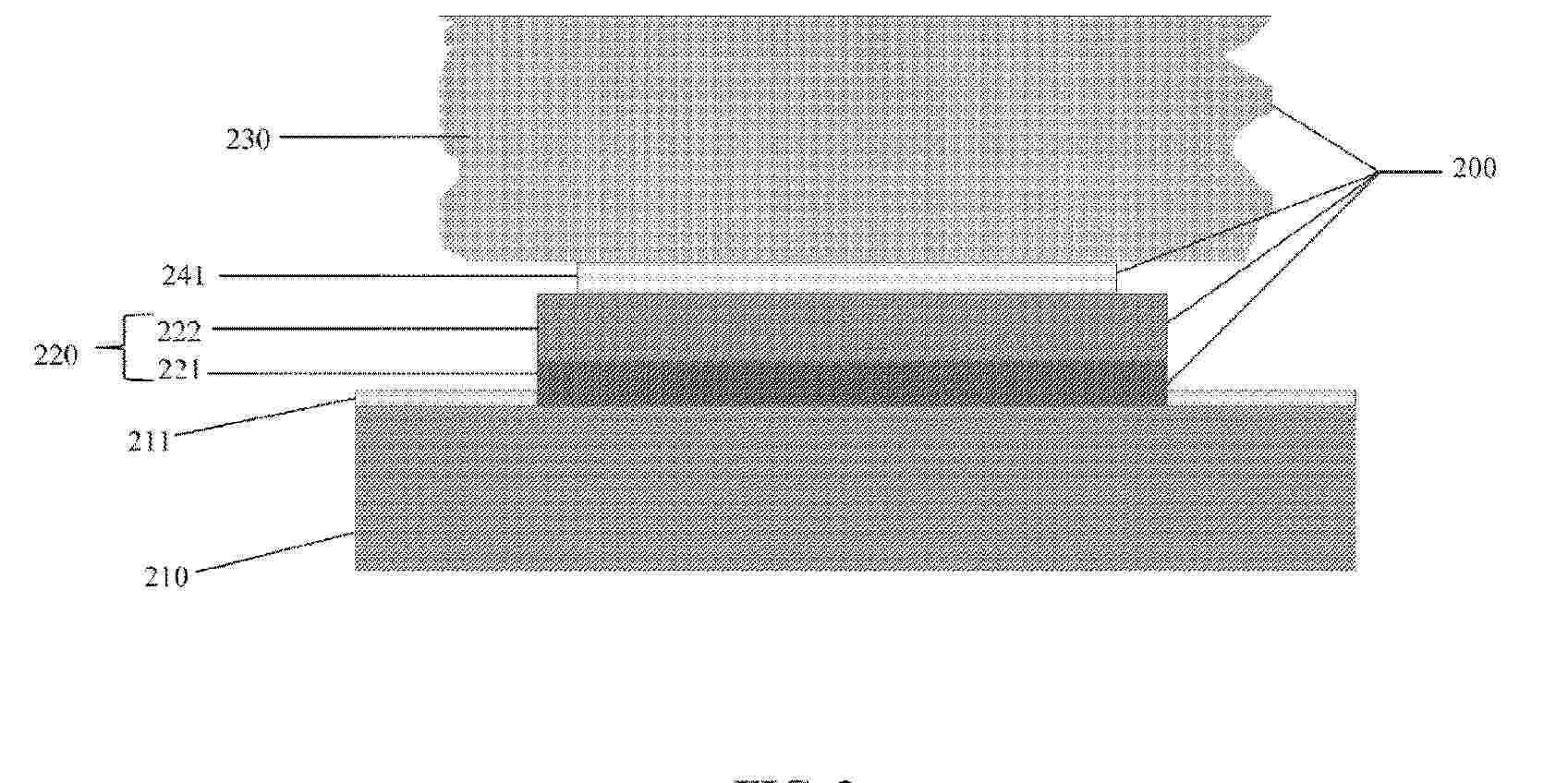
A conductive multilayer stack or a conductive multilayer line useful as a metallization layer in photovoltaics as well as other devices; solar cells having a conductive multilayer stack or line; solar modules having such cells; and methods of forming a conductive multilayer stack or line. The conductive multilayer stack or line having a metal layer including copper (Cu) or coated aluminum; a silver contact layer; and a solderable layer between, and contacting, the metal layer and the silver contact layer.
Resumen de: WO2025097074A1
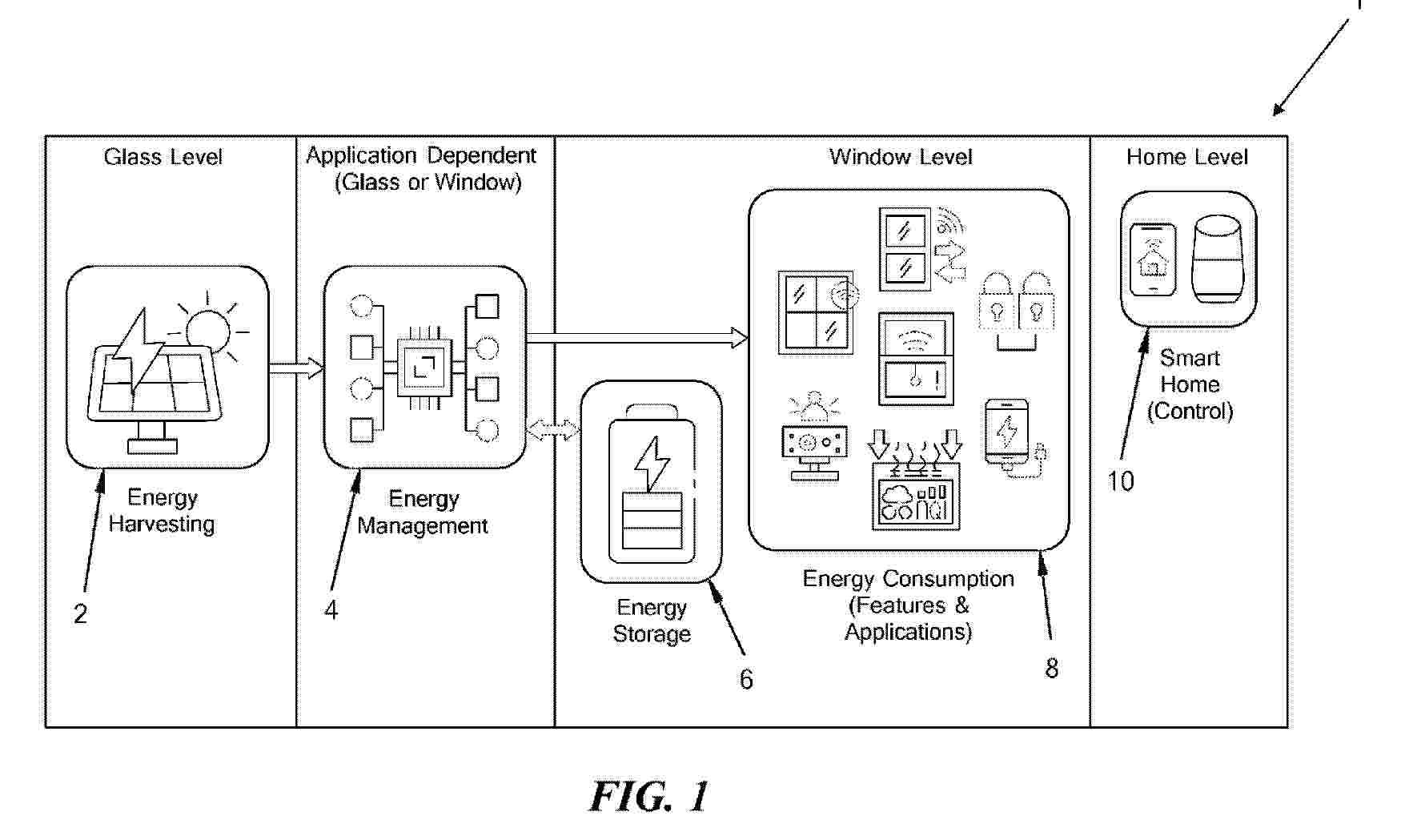
Illustrative embodiments present a self-contained window system that includes a solar-generating glass window, pods that contain components, an energy storage device, and electrical circuits that distribute electrical power that is generated by the solar-generating glass and distributed to the components and the energy storage device. The self-contained window system is secured to a structure that may be a window frame, a glazing bead, or the like. In illustrative embodiments, the pods are secured inside of the structure, while in other illustrative embodiments the pods are secured on the outside of the structure. Regardless of whether the pods are secured inside or outside of structure, the components in the pods are accessible and easy to maintain. The pods and components can be conveniently exchanged and upgraded.
Resumen de: EP4804778A2
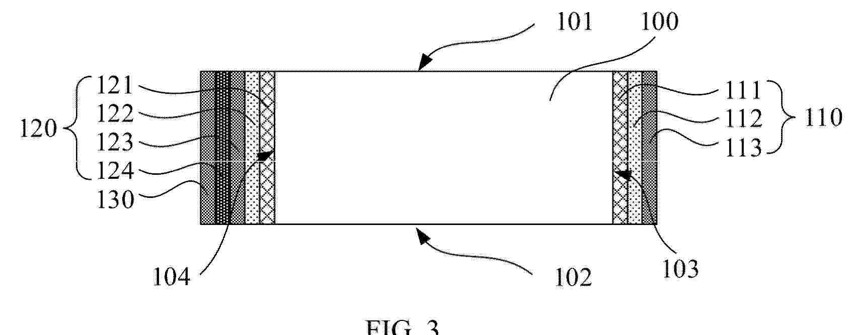
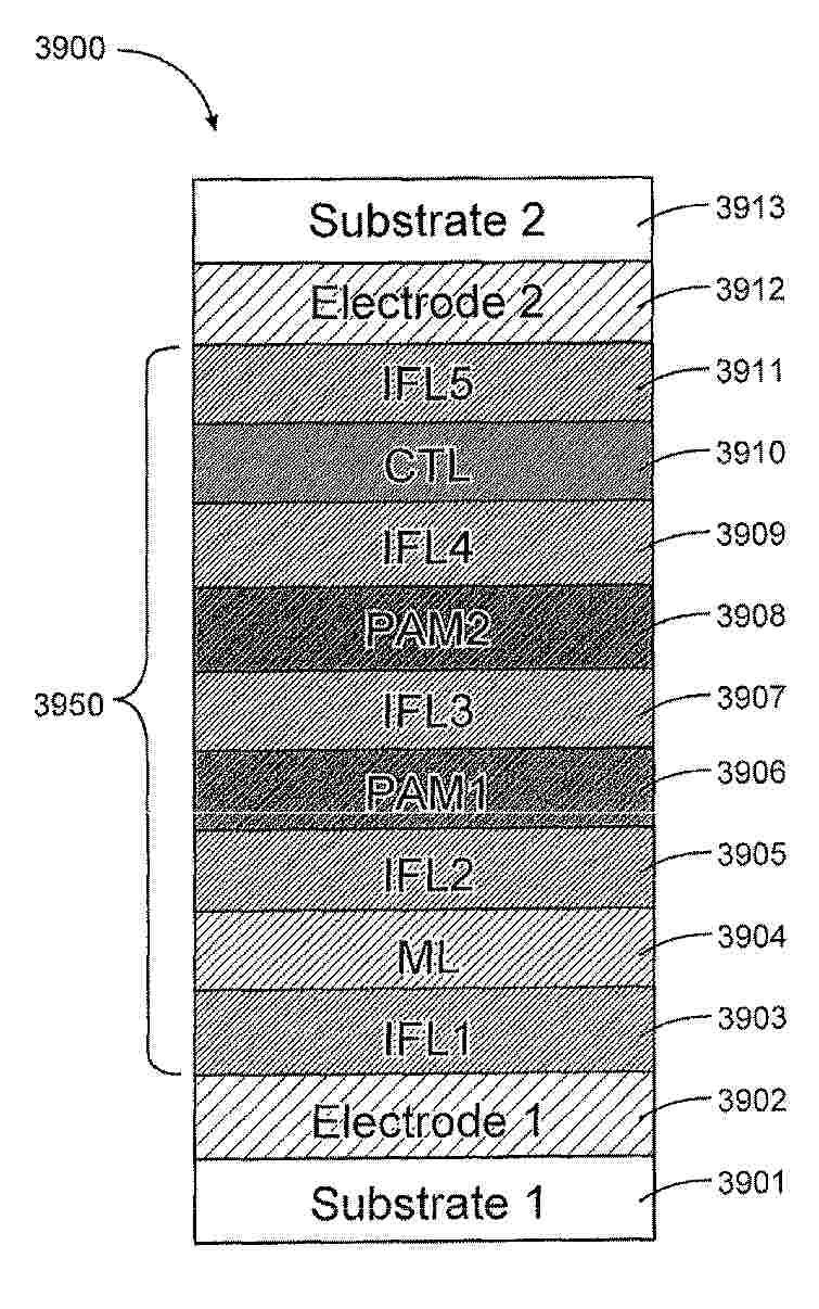
Photovoltaic devices such as solar cells, hybrid solar cell-batteries, and other such devices may include an active layer disposed between two electrodes, the active layer having perovskite material and other material such as mesoporous material, interfacial layers, thincoat interfacial layers, and combinations thereof. The perovskite material may be photoactive. The perovskite material may be disposed between two or more other materials in the photovoltaic device. Inclusion of these materials in various arrangements within an active layer of a photovoltaic device may improve device performance. Other materials may be included to further improve device performance, such as, for example: additional perovskites, and additional interfacial layers.
Resumen de: EP4804765A1
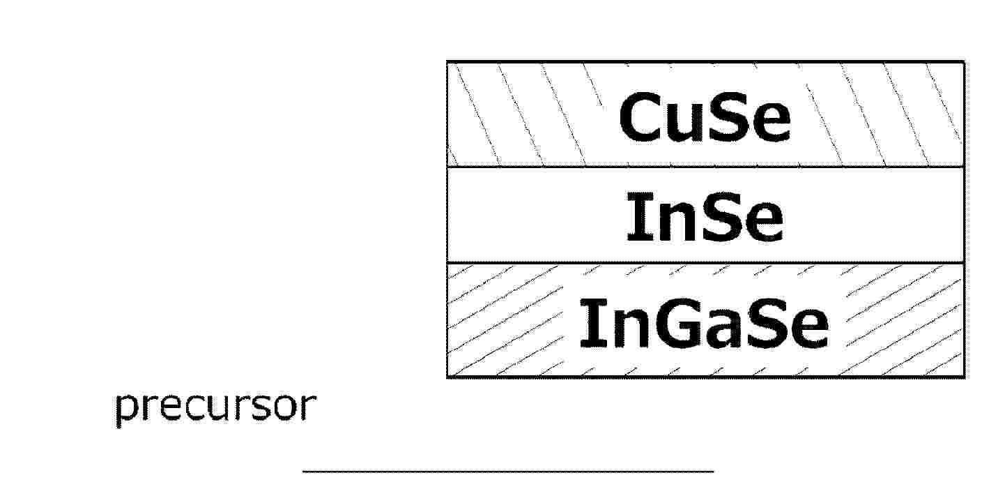
0001 An object of the present invention is to provide a highly productive method for manufacturing a solar cell that achieves high performance. The object can be achieved by a method for manufacturing a solar cell, including: a precursor formation step of forming a precursor including an InGaSe layer, a CuSe layer, and an InSe layer; and a crystallization step of obtaining a crystallized light-absorbing layer by heating the precursor.
Nº publicación: EP4802612A1 09/09/2026
Solicitante:
CIEL ET TERRE INT [FR]
Ciel et Terre International
Resumen de: WO2025093841A1
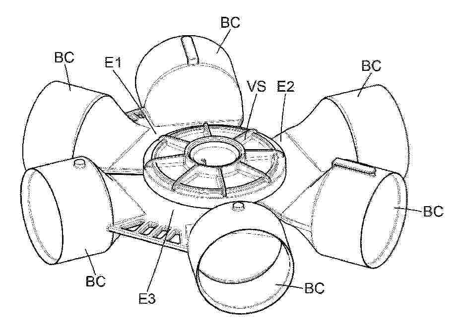
The present disclosure relates to a floating modular assembly (1) comprising at least two floating devices (D1, D2, D3) and a connecting system, configured to mechanically connect the at least two floating devices, the connecting system comprising - a first coupling element (E1), rigidly attached to and projecting laterally from a first floating device (D1) - a second coupling element (E2), rigidly attached to and projecting laterally from the second floating device (D2) - a removable locking system, configured to connect the first coupling element to the second coupling element.
 BOPI
BOPI
 Sede Electrónica