Si deseas distinguir tus productos, servicios o ambos de los de otra empresa, es posible que necesites una marca o nombre comercial. Descubre qué son, en qué consiste su procedimiento de registro y qué implica.

Información sobre los plazos de presentación de solicitudes de transformación de marcas de la Unión Europea en marca nacional española. Más información


Si tienes un nuevo dispositivo, producto o procedimiento que resuelva un problema técnico o tenga una ventaja práctica, existen distintas formas de protegerlo en España y en otros países. Descubre cómo hacerlo.

¿Tu innovación reside en la estética, la ornamentación o la apariencia de tu producto? Protégela mediante un diseño industrial. Descubre qué derechos confiere el registro y cómo realizar la tramitación.

Las indicaciones geográficas protegen el nombre de un producto originario de una zona geográfica, a la cual le debe una determinada calidad, reputación u otra característica. Descubre qué son, en qué consiste su procedimiento de registro y qué beneficios conceden.

Las patentes publicadas en todo el mundo son una valiosa fuente de información científica, técnica y comercial.

Si eres emprendedor/a o una empresa y quieres potenciar y mejorar la rentabilidad de tu negocio protegiendo de forma adecuada los activos intangibles de tu organización, en este espacio encontrarás lo necesario.


 228
resultados
228
resultados
 Última actualización
14/07/2026 [08:33:00]
Última actualización
14/07/2026 [08:33:00]


 Resultados 25 a 50 de 228

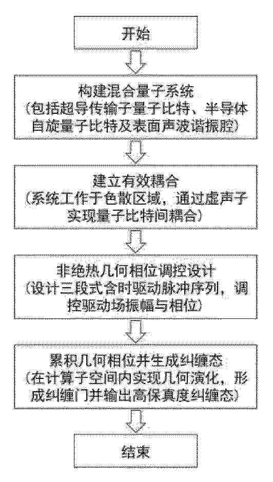
Resumen de: CN122366694A
本发明公开了一种基于几何相位的混合量子系统纠缠生成方法,该方法先构建含超导传输子量子比特、半导体自旋量子比特和表面声波谐振腔的混合量子系统,以谐振腔内虚声子为量子换能器,将系统置于色散区域实现两量子比特有效耦合;再基于非绝热几何相位调控,设计三段式驱动脉冲序列形成纠缠门;最后控制驱动场振幅和相位,累积几何相位生成高保真度纠缠态。本发明实现了混合系统紧凑片上集成,100纳秒内可形成保真度≥0.96的纠缠门,量子态转移保真度达0.966以上,对参数波动和环境耗散鲁棒性优异,方案易实现且可扩展至同类混合量子系统,能够为可扩展量子信息处理提供技术支撑。

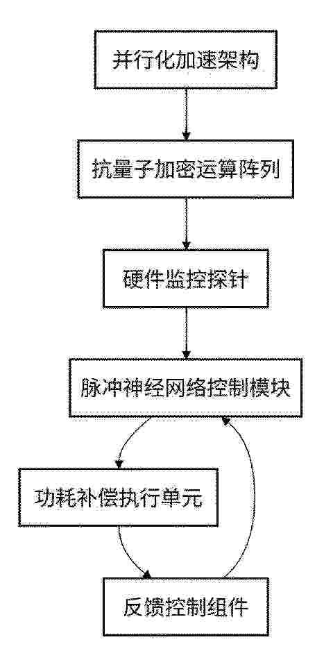
Resumen de: CN122372180A
本发明涉及信息安全与抗量子计算领域,公开了一种基于硬件加速的抗量子加密算法并行化实现方法及系统。该方法包括:配置并行化抗量子加密核心运算阵列;部署模拟生物神经元随机放电行为的脉冲神经网络控制模块,并连接功耗补偿执行单元;监测关键运算周期并激活该模块;利用其生成的非周期性随机脉冲驱动功耗扰动,深度融合瞬时功耗与噪声;通过反馈机制动态调整神经元参数,使总功耗呈现类生物神经电信号的随机特征。本发明通过上述方案,将加密功耗轨迹伪装为随机噪声,在不牺牲运算效能的前提下,抵御差分功耗分析等物理攻击,提升抗量子加密系统的物理层安全性与能效比。
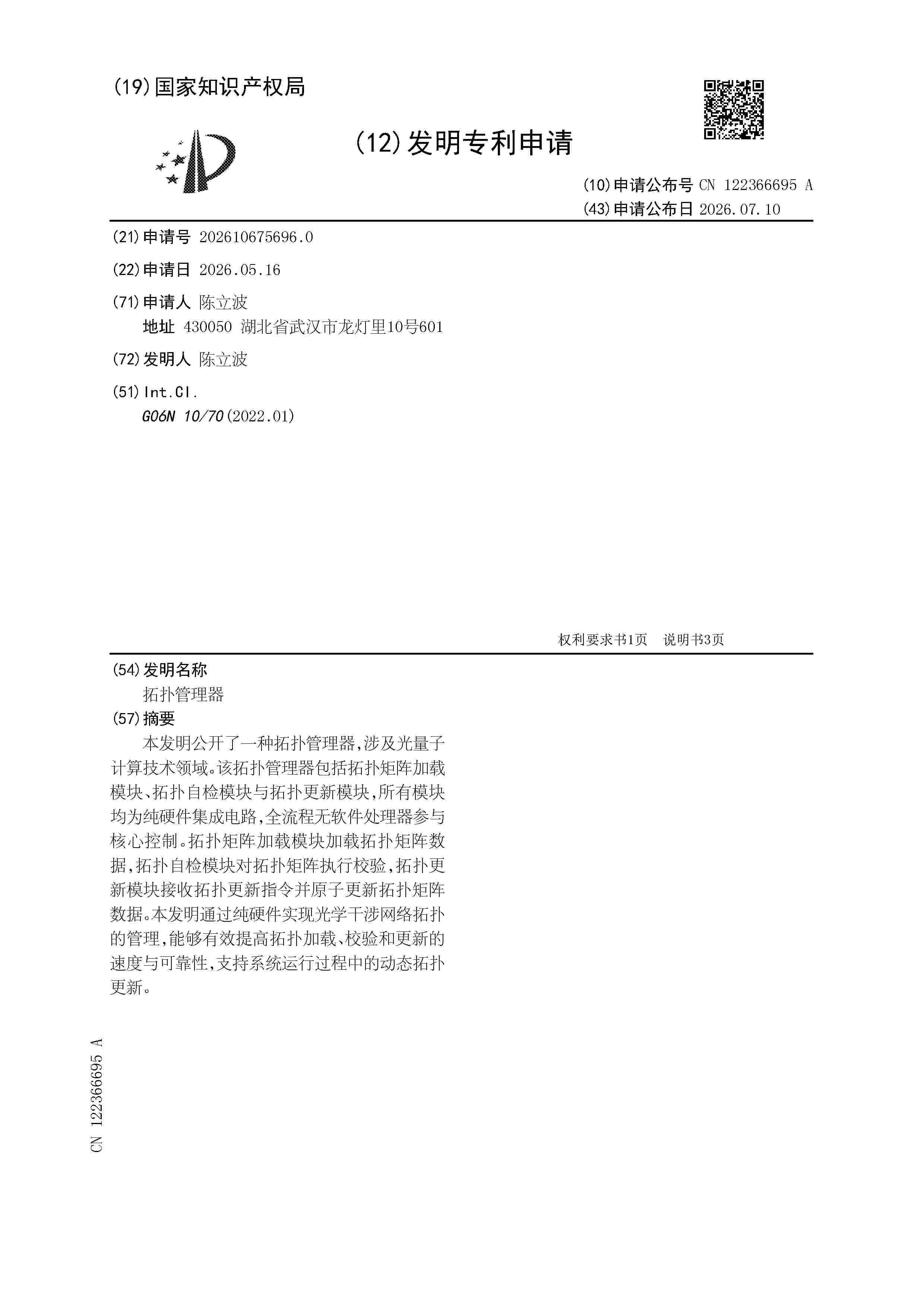
Resumen de: CN122366695A
本发明公开了一种拓扑管理器,涉及光量子计算技术领域。该拓扑管理器包括拓扑矩阵加载模块、拓扑自检模块与拓扑更新模块,所有模块均为纯硬件集成电路,全流程无软件处理器参与核心控制。拓扑矩阵加载模块加载拓扑矩阵数据,拓扑自检模块对拓扑矩阵执行校验,拓扑更新模块接收拓扑更新指令并原子更新拓扑矩阵数据。本发明通过纯硬件实现光学干涉网络拓扑的管理,能够有效提高拓扑加载、校验和更新的速度与可靠性,支持系统运行过程中的动态拓扑更新。
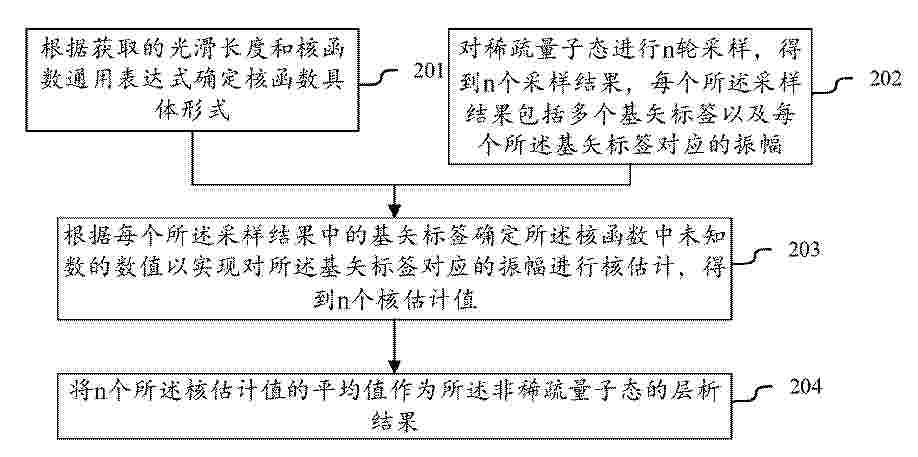
Resumen de: CN122366692A
本申请实施例公开了一种非稀疏量子态数据层析方法及相关装置,该方法包括:根据获取的光滑长度和核函数通用表达式确定核函数具体形式,以及对稀疏量子态进行n轮采样,得到n个采样结果,每个所述采样结果包括多个基矢标签以及每个所述基矢标签对应的振幅,所述n为大于0的正整数;根据每个所述采样结果中的基矢标签确定所述核函数中未知数的数值以实现对所述基矢标签对应的振幅进行核估计,得到n个核估计值;将n个所述核估计值的平均值作为所述非稀疏量子态的层析结果。采用本申请实施例,有利于降低非稀疏量子态数据的层析复杂度,从而提高非稀疏量子态数据的提取速度,降低非稀疏量子态数据层析过程中存储资源需求。
Resumen de: GB2636580A
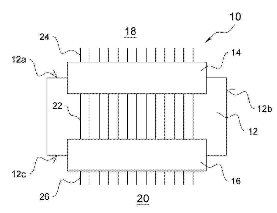
A vacuum feedthrough 10 providing an electrical connection from ambient pressure into a vacuum chamber 18 comprises: a first wall (12a, Fig. 1) at least partially connected to or part of the vacuum chamber; a second wall (12c) connected to the first wall by one or more sidewalls (12b), thereby defining an internal volume 12; a first electrical feedthrough 14 arranged in the first wall providing one or more electrical connections (24) through the first wall in a vacuum tight manner; a second electrical feedthrough 16 arranged in the second wall providing one or more electrical connections 26 through the second wall in a vacuum tight manner, the one or more electrical connections of the first electrical feedthrough being connected with respective electrical connections of the second electrical feedthrough; wherein the internal volume is a vacuum. The internal volume may be connected to a vacuum pump 34 or an inner surface of one or more of said walls may be covered with a NEG material.
Resumen de: US20260195630A1
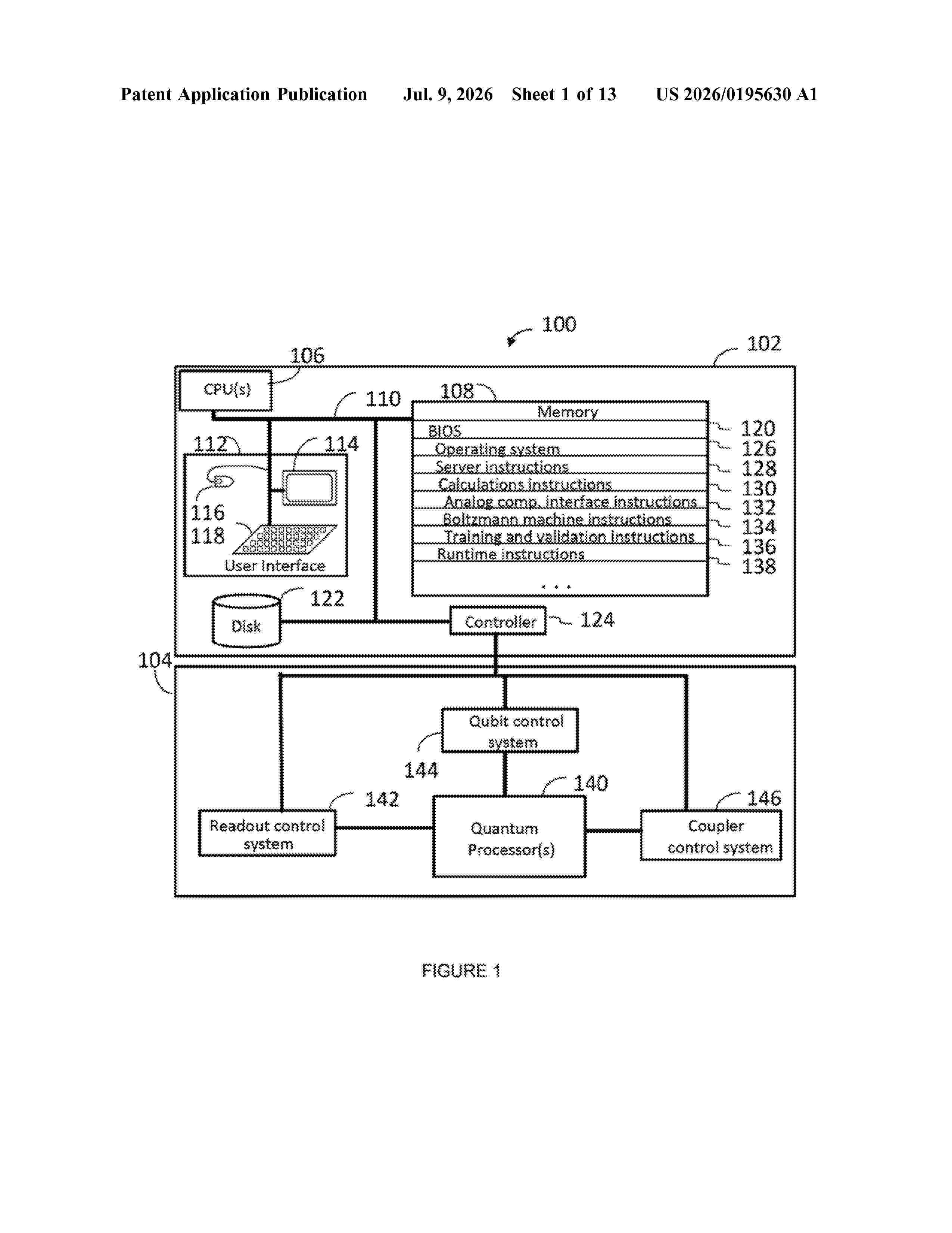
A computational method via a hybrid processor comprising an analog processor and a digital processor includes determining a first classical spin configuration via the digital processor, determining preparatory biases toward the first classical spin configuration, programming an Ising problem and the preparatory biases in the analog processor via the digital processor, evolving the analog processor in a first direction, latching the state of the analog processor for a first dwell time, programming the analog processor to remove the preparatory biases via the digital processor, determining a tunneling energy via the digital processor, determining a second dwell time via the digital processor, evolving the analog processor in a second direction until the analog processor reaches the tunneling energy, and evolving the analog processor in the first direction until the analog processor reaches a second classical spin configuration.
Resumen de: US20260195450A1
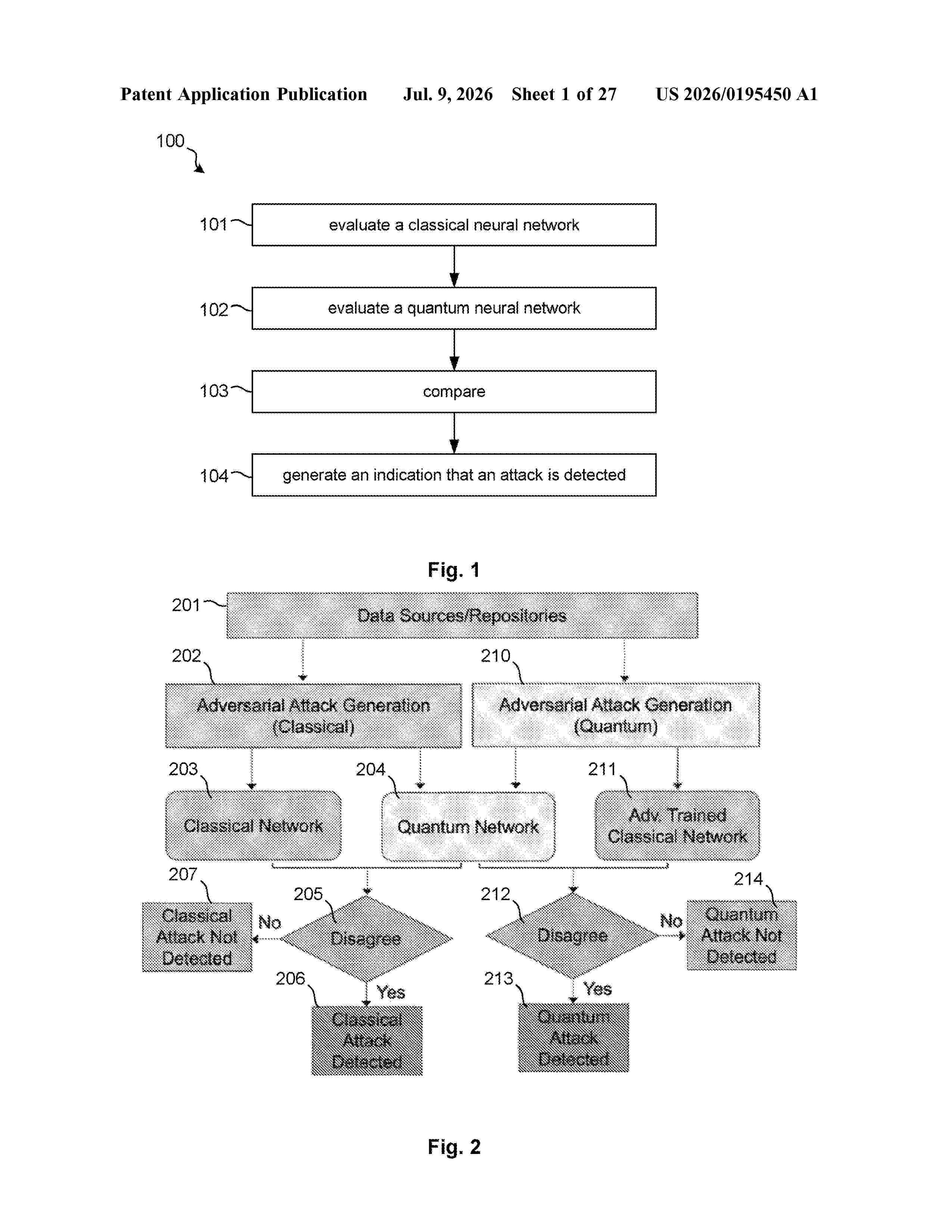
This disclosure relates to a method for detecting an attack on a machine learning system. A classical neural network comprises a first output indicative of a first classification by the classical neural network and a quantum neural network comprises a second output indicative of a second classification of the input data by the quantum neural network. The method comprises comparing the first output to the second output; and responsive to the first output being different to the second output, generating an indication that an attack is detected.
Resumen de: US20260195625A1
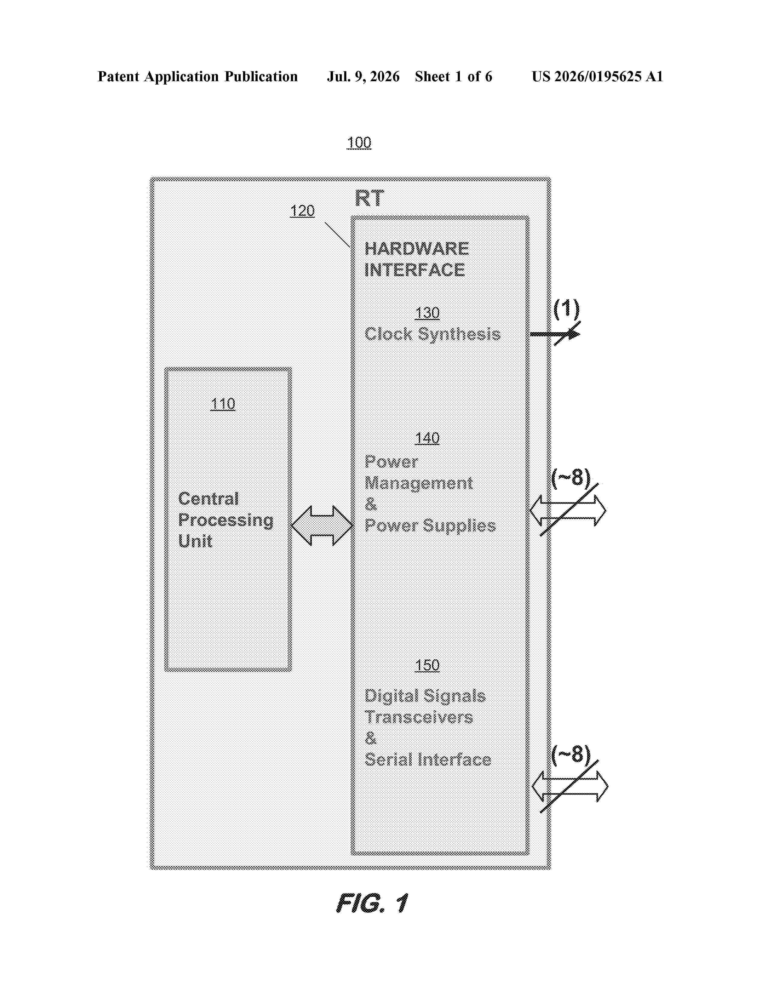
A system for implementing a hybrid cryogenic electronic architecture is disclosed. The system comprises: a cryostat system operable to provide a first cryogenic temperature and a second cryogenic temperature; a quantum computing module comprising a plurality of quantum bit circuits capable of superconducting at the first cryogenic temperature; a CMOS circuitry module enclosed by the cryostat at the second cryogenic temperature and structured to support complementary metal-oxide-semiconductor (CMOS) circuits configured to interface with SFQ logic circuitry to allow control signals and quantum bit signals to be transferred therebetween; and an ambient temperature or room temperature (RT) control module operable to provide input signals to the CMOS circuitry module and to receive therefrom readout signals associated with quantum states of the plurality of quantum bit circuits.
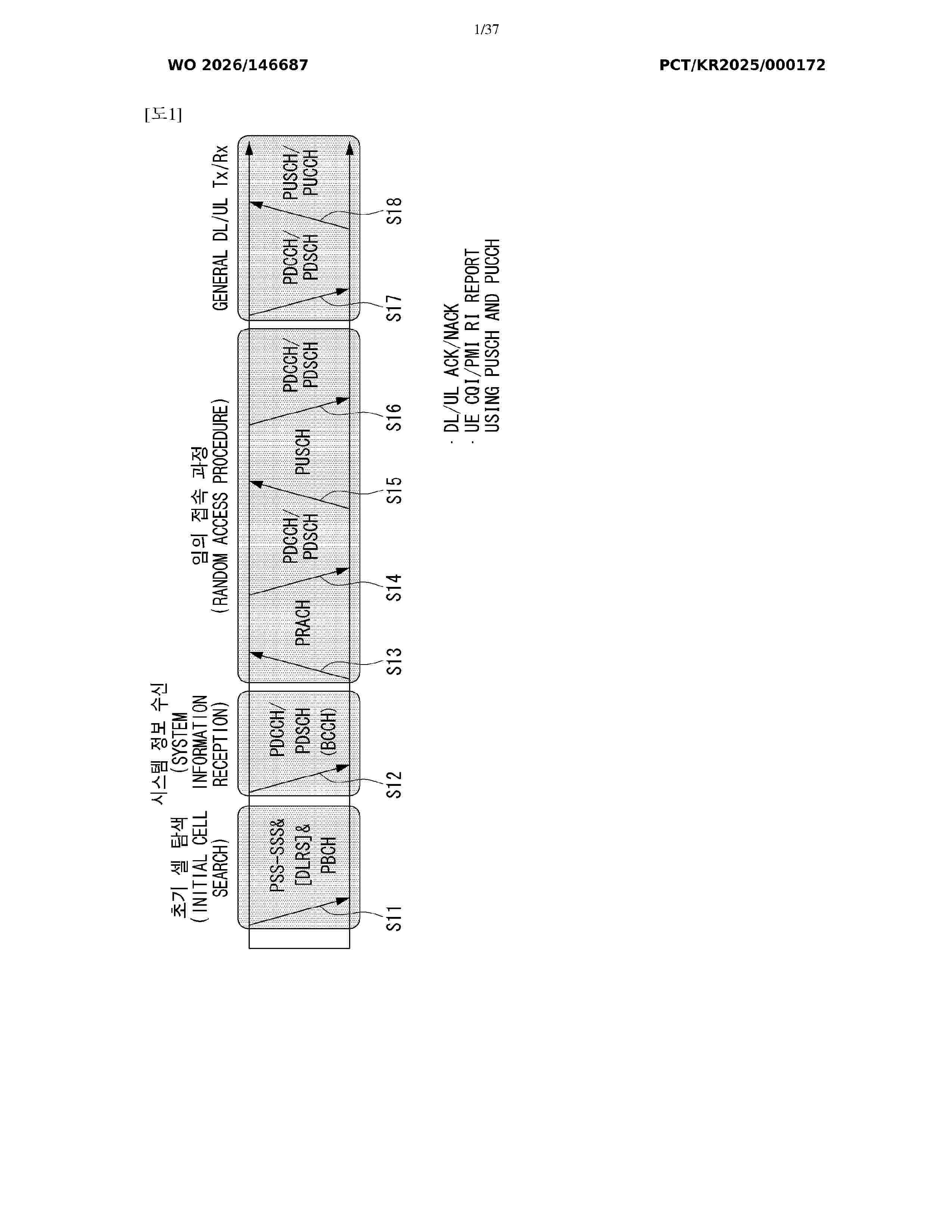
Resumen de: WO2026146687A1
According to various embodiments of the present disclosure, a method performed by a first node is provided, the method comprising the steps of: transmitting, to a second node, information related to initial fidelity and target fidelity of an Einstein-Podolsky-Rosen (EPR) pair, the number of rounds in which an entanglement distillation protocol (EDP) is performed, and an EDP type; transmitting, to the second node, information related to the entanglement state of the EPR pair; determining an optimal EDP mode for optimal EPR yield; transmitting, to the second node, information about the optimal EDP mode for the optimal EPR yield; and performing the EDP on the basis of the optimal EDP mode.
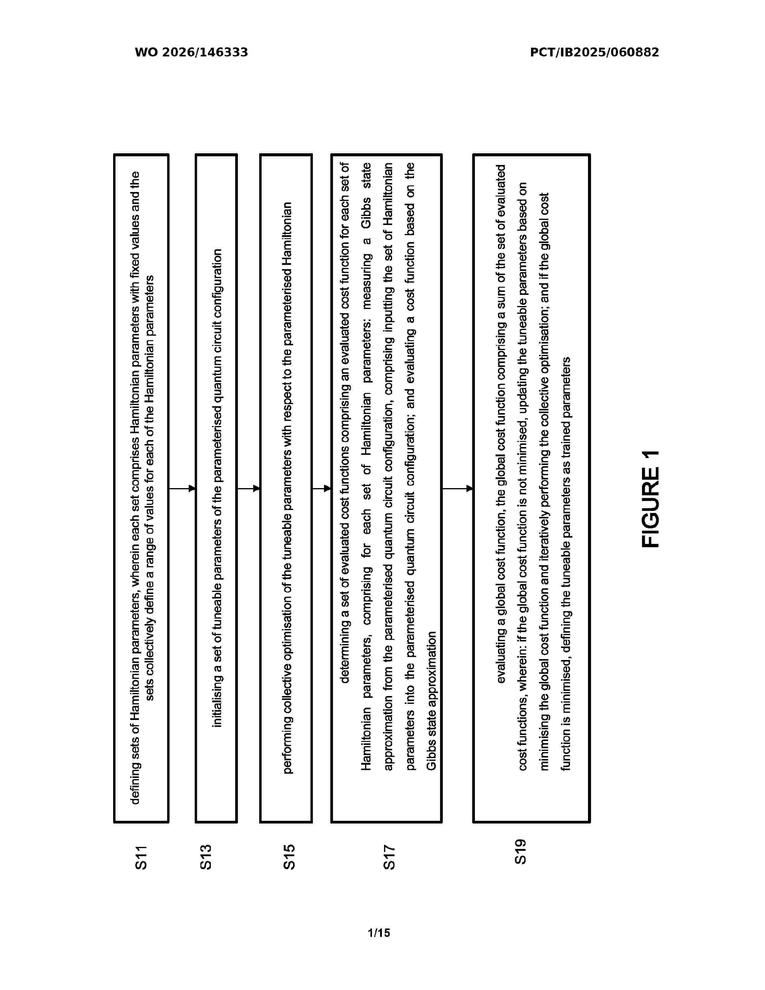
Resumen de: WO2026146333A1
There is provided a computer-implemented hybrid variational method of training a parametrised quantum circuit configuration to perform Gibbs state generation of a parametrised Hamiltonian.
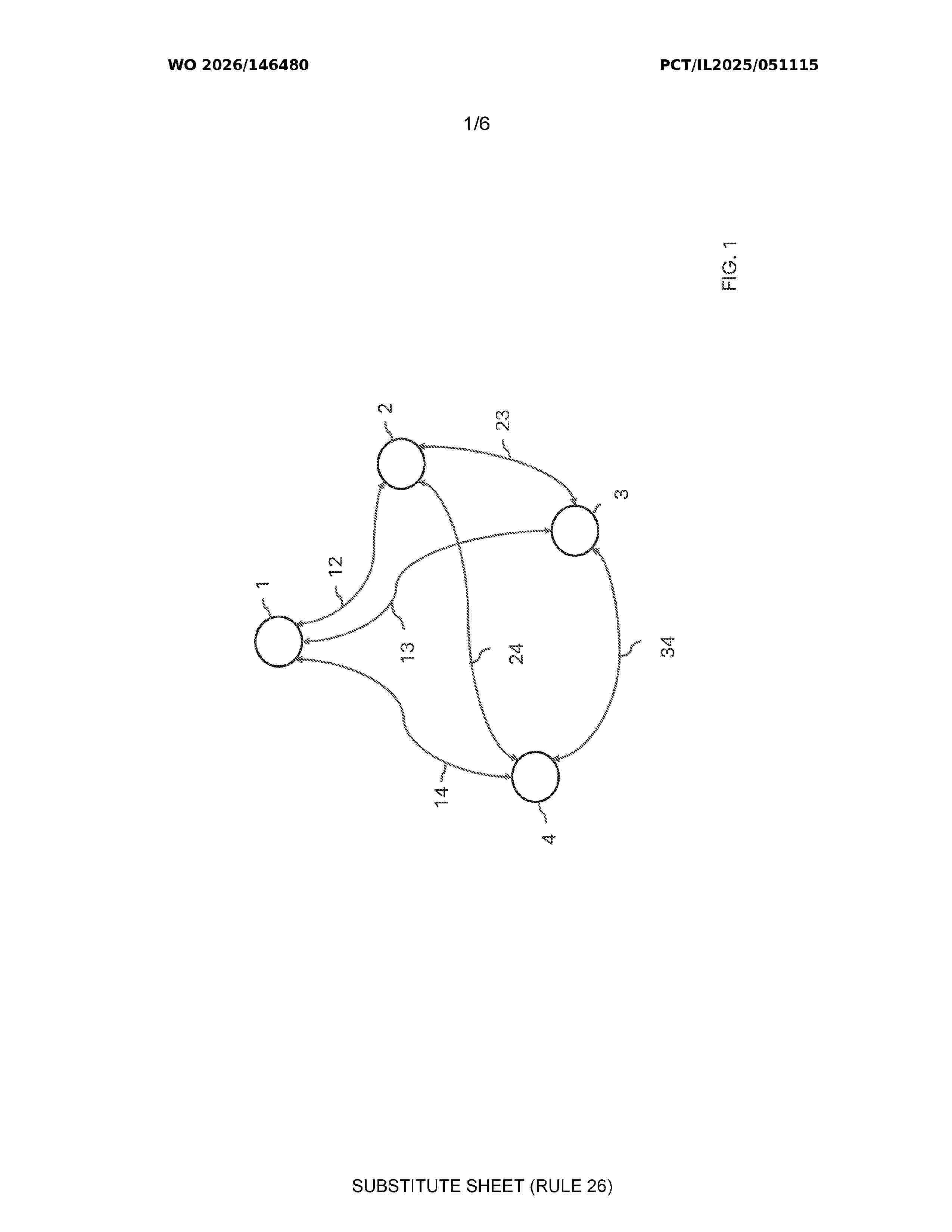
Resumen de: WO2026146480A1
A quantum computing method and system optimize technical processes involving the Traveling Salesman Problem (TSP). The method initializes N quantum registers, each corresponding to a task position and comprising N qubits. A W state is generated in each register, representing an equally distributed superposition of quantum states. Controlled operations encode the technical costs of transitions between tasks as phase shifts between qubits in adjacent registers. Optionally, penalty phase shifts are applied to qubits in different registers corresponding to the same task. The state of the quantum registers is measured, and the process is repeated over multiple trials to identify the most frequently measured state, providing a target task sequence. The system includes quantum registers, a superposition generator, a phase encoder, a measurement unit, and a processor to perform the method. Applications include manufacturing, data transfer, and genome sequencing, optimizing technical costs such as energy expenditure, bandwidth consumption, and DNA segment overlap.
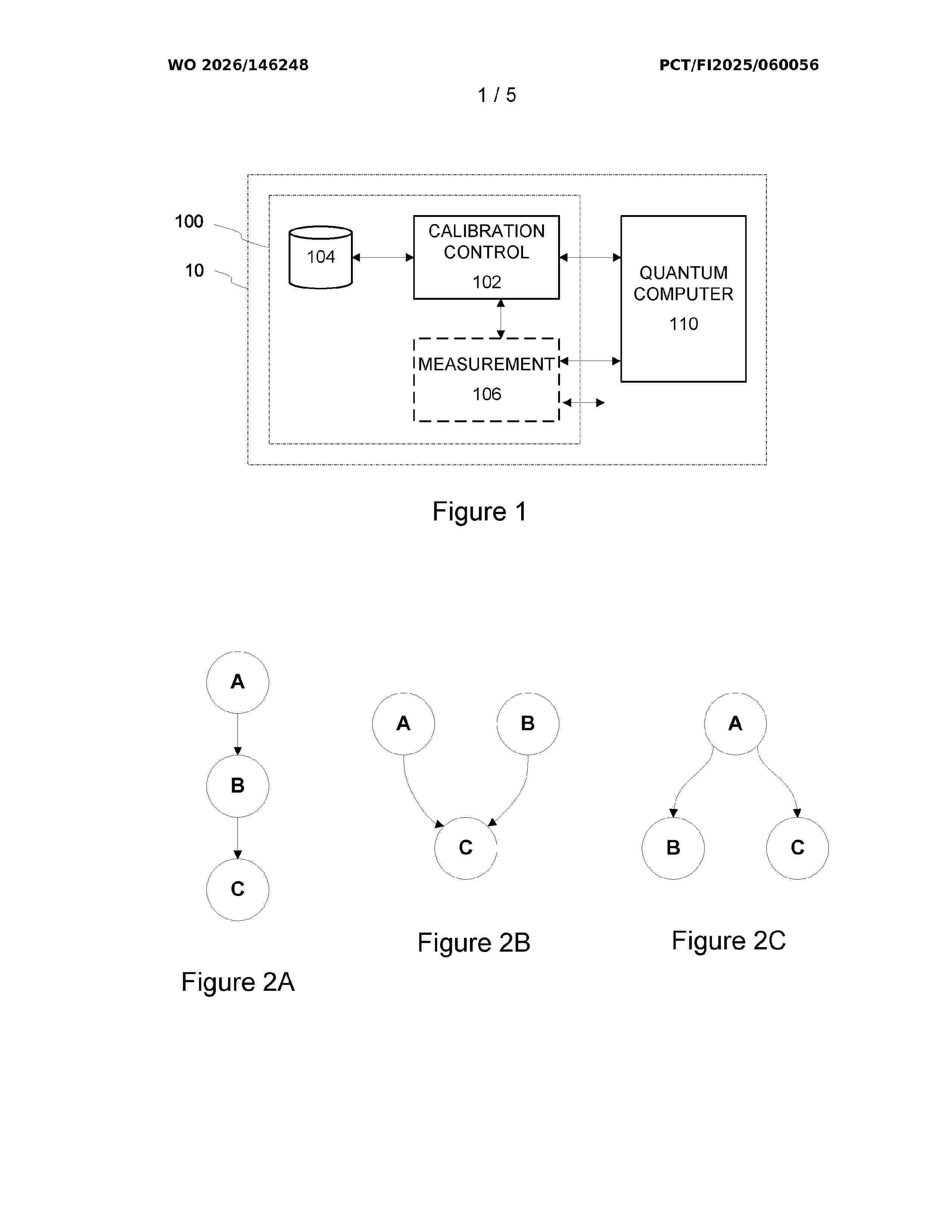
Resumen de: WO2026146248A1
According to an example embodiment, a method (200) for controlling calibration of a quantum computer (110) is provided, the method (200) to be carried out by a calibration control apparatus and comprising: modeling (202) dependencies between a plurality of calibration tasks pertaining to the quantum computer (110) by a directed calibration graph comprising a plurality of nodes that each represent a respective one of said plurality of calibration tasks and a plurality of directed edges that each connect a pair of nodes and indicate a dependency of a calibration task represented by the head of the respective edge on a calibration task represented by the tail of the respective edge; and carrying out (204) a calibration procedure via executing the plurality of nodes in a dependency order defined in the calibration graph, where execution of each node comprises carrying out the calibration task represented by the respective node, wherein the plurality of nodes may comprise one or more adaptation nodes, where execution of an adaptation node further comprises deriving (206) a node status value that indicates either successful execution or an error condition and where the calibration procedure proceeds from the respective adaptation node to a subsequent node selected in dependence of the node status value.
Resumen de: WO2026148345A1
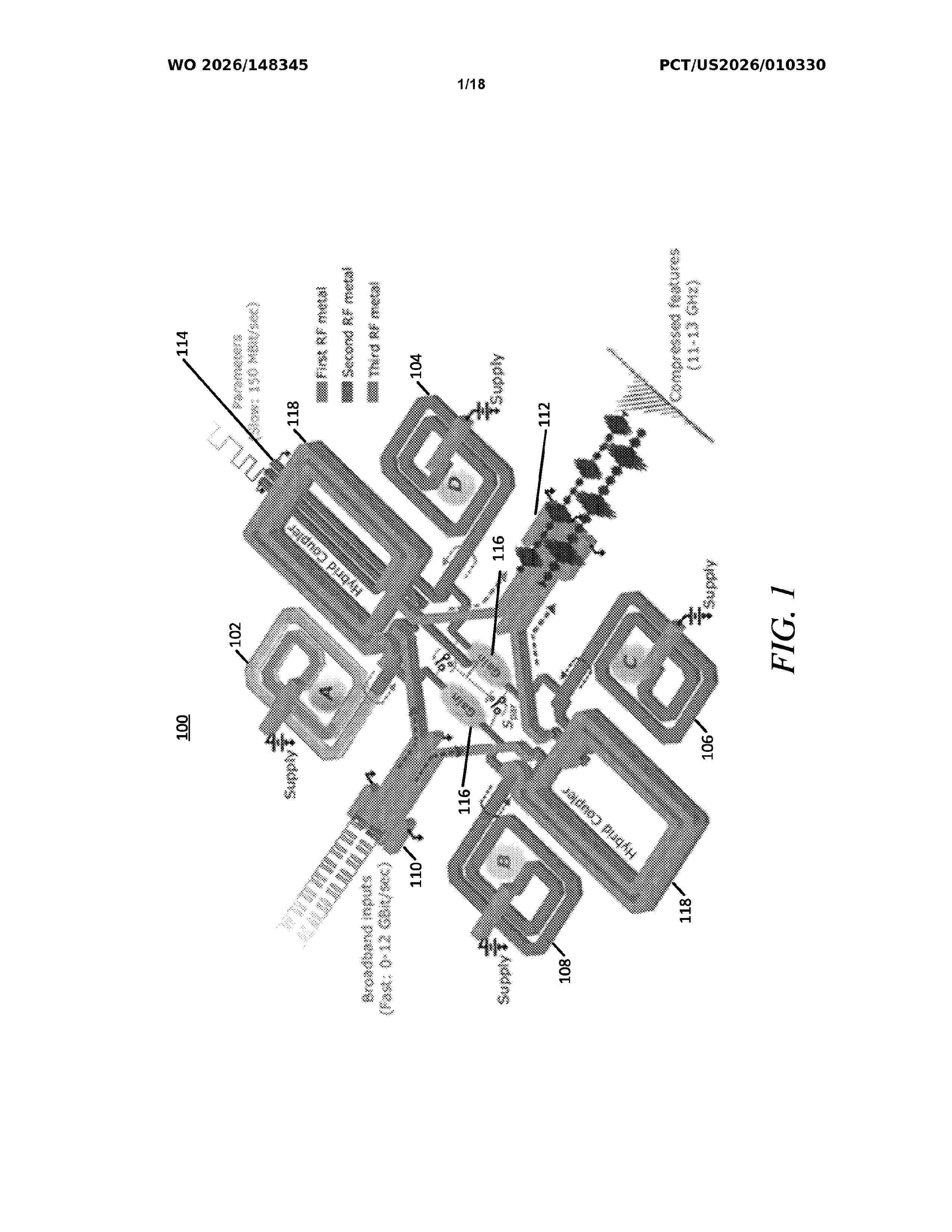
A signal modification unit configured for processing high-bandwidth signals includes at least one signal input configured to receive a high-bandwidth signal. The signal modification unit includes a tunable control component configured to adjust one or more parameters for modifying the high-bandwidth signal, wherein the one or more parameters are associated with nonlinear modification of the high-bandwidth signal. The signal modification unit includes one or more waveguide components configured to modify the high-bandwidth signal to generate a modified signal based in part upon the one or more parameters. The signal modification unit includes at least one signal output configured to provide the modified signal as an output of the signal modification unit. The signal modification unit allows for feature extraction of spectral bands and may be used to replace parts of digital neural networks.
Resumen de: WO2026146666A1
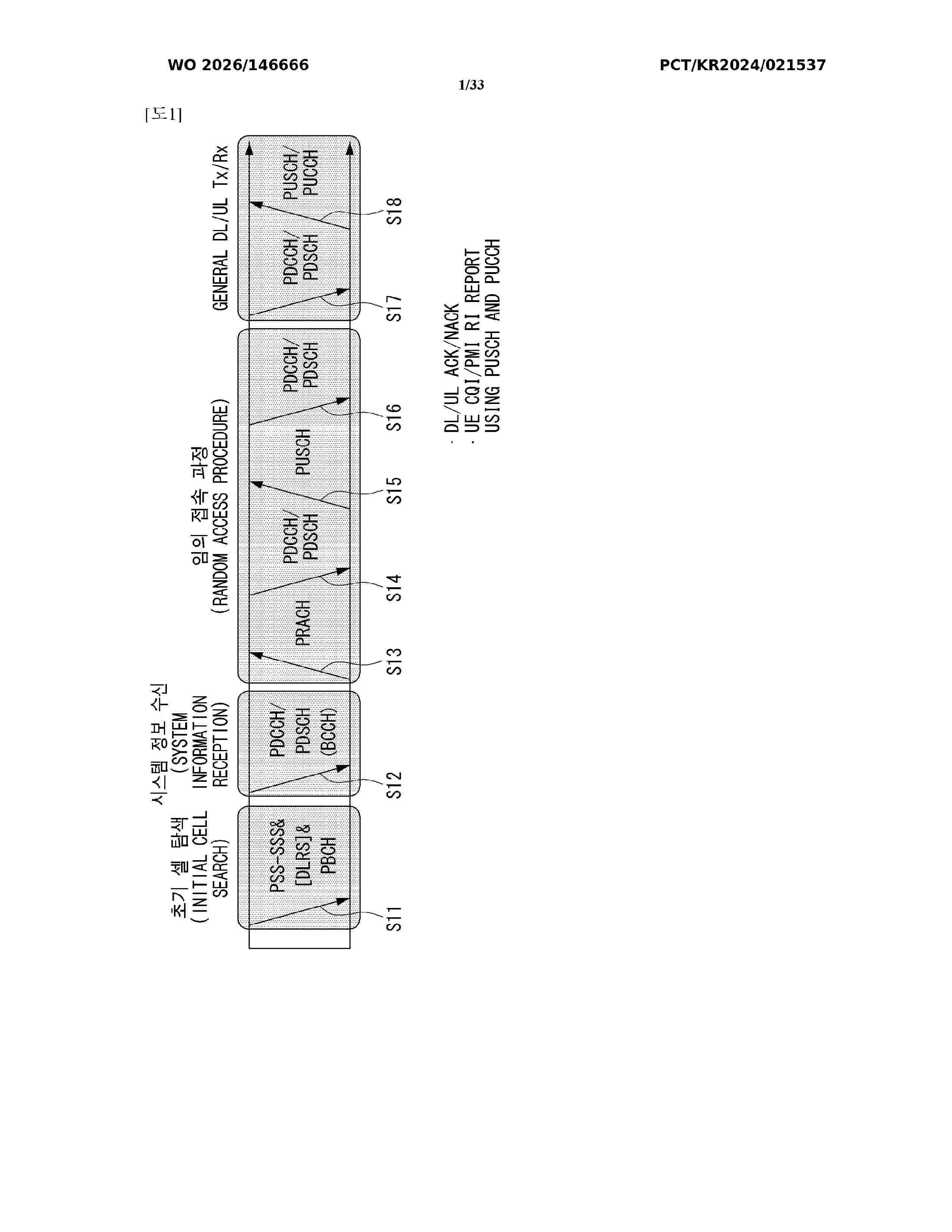
The present disclosure relates to an apparatus and method for performing an entanglement percolation-based entanglement routing strategy using local information in a quantum communication system. Specifically, the present disclosure relates to an apparatus and method in which each intermediate node involved in distributing remote entanglement between any two distant transmitting and receiving nodes on the basis of entanglement percolation in a quantum communication system determines a local operation and classical communication (LOCC) strategy thereof on the basis of local information. The present disclosure relates to an apparatus and method for determining an operation mode of a specific node as one of a repeater mode, a vertex mode, or a hybrid mode using only information between the specific node and neighboring nodes, and performing entanglement routing on the basis of an LOCC strategy corresponding to each mode.
Resumen de: US20260195212A1
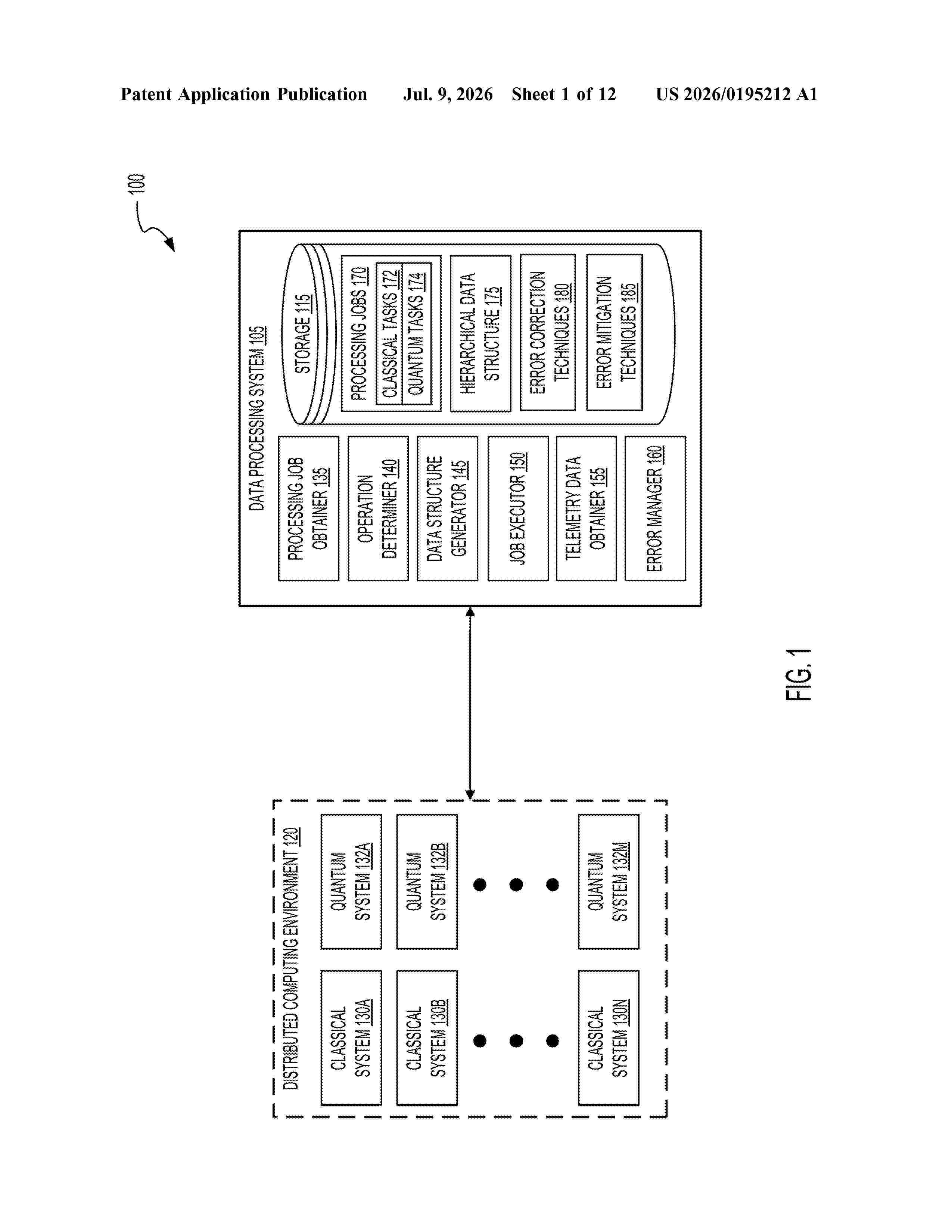
Systems and methods for dynamic error resolution in hybrid quantum-classical computing environments are disclosed. A system can obtain telemetry data corresponding to a processing job. The system can determine that an error resolution technique is to be applied to the quantum portion of the processing job. The system can select, for a quantum portion of the processing job, the error resolution technique from a plurality of error correction techniques and a plurality of error mitigation techniques. The system can update a hierarchical data structure representing the processing job as at least a set of nodes. The hierarchical data structure can be updated to include the error resolution technique in association with a respective node of the hierarchical data structure representing the quantum portion of the processing job.
Resumen de: AU2025211815A1
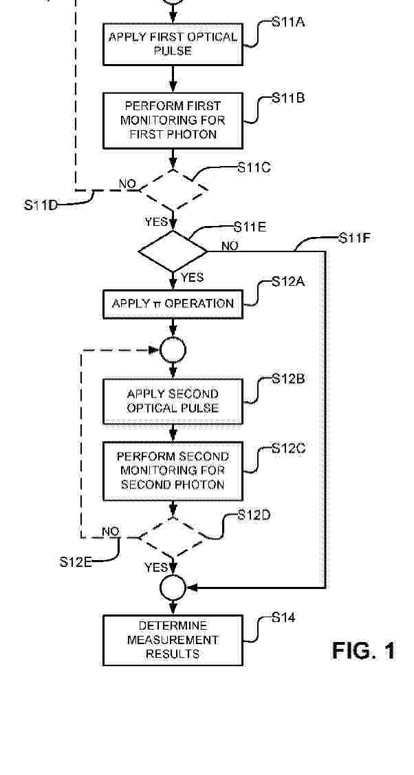
Methods and apparatus for measuring quantum systems involve: applying first optical pulses to the quantum system and monitoring for a first resulting photon after each first optical pulse; in response to detecting one or more first resulting photons, performing a π operation on the quantum system; and, after performing the π operation, applying second optical pulses to the quantum system and monitoring for a second resulting photon after each second optical pulse. The first and second optical pulses comprise a wavelength corresponding to a transition from a first basis state of the quantum system to an excited state. A measurement result is determined based on results of the monitoring.
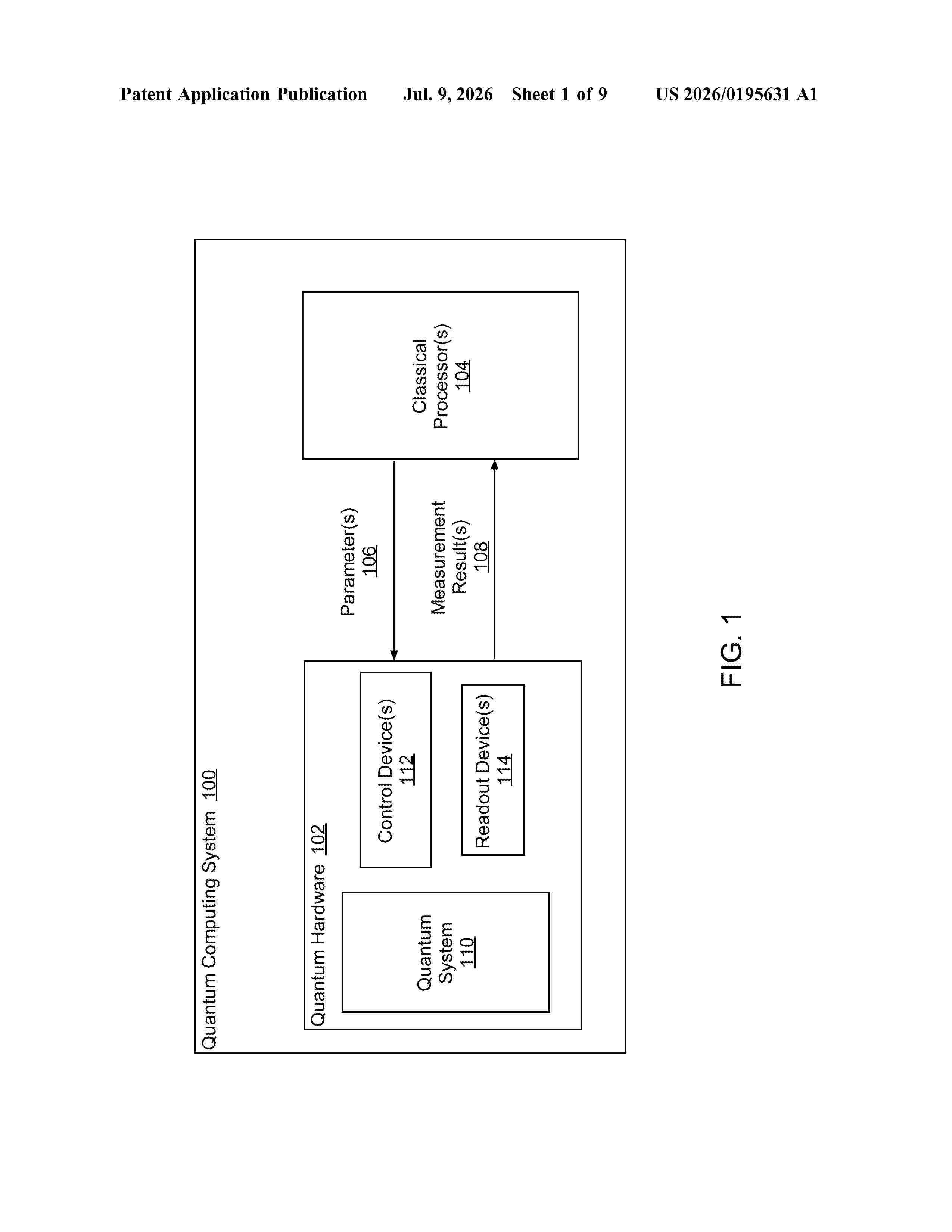
Resumen de: US20260195631A1
0000 Systems and methods for tracking errors in a quantum computing system are provided. In one example, a method can include matching data associated with one or more detection events associated with a quantum computing system using a successive pattern structure comprising a plurality of processing layers. Each processing layer in the plurality of processing layers can be associated with a pattern including a plurality of sections. Each section can be associated with a processing unit operable to match one or more detection events near a center of the section. The method can include tracking one or more errors of a quantum computing system based at least in part on a matching of one or more detection events.
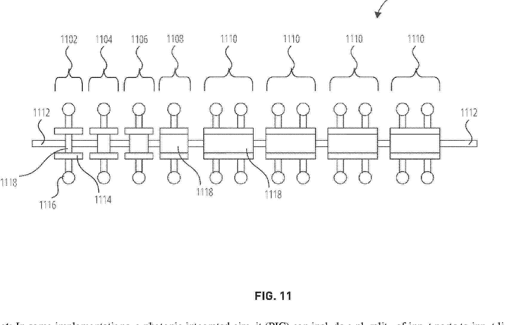
Resumen de: AU2024409733A1
In some implementations, a photonic integrated circuit (PIC) can include a plurality of input ports to input light, such as quantum light (e.g., single photons) or bright light. In addition, the PIC may include a waveguide network that includes a crossing network to interfere the light. The light can be phase shifted using segmented phase shifters. The photonic integrated circuit can further include output ports to output the light.
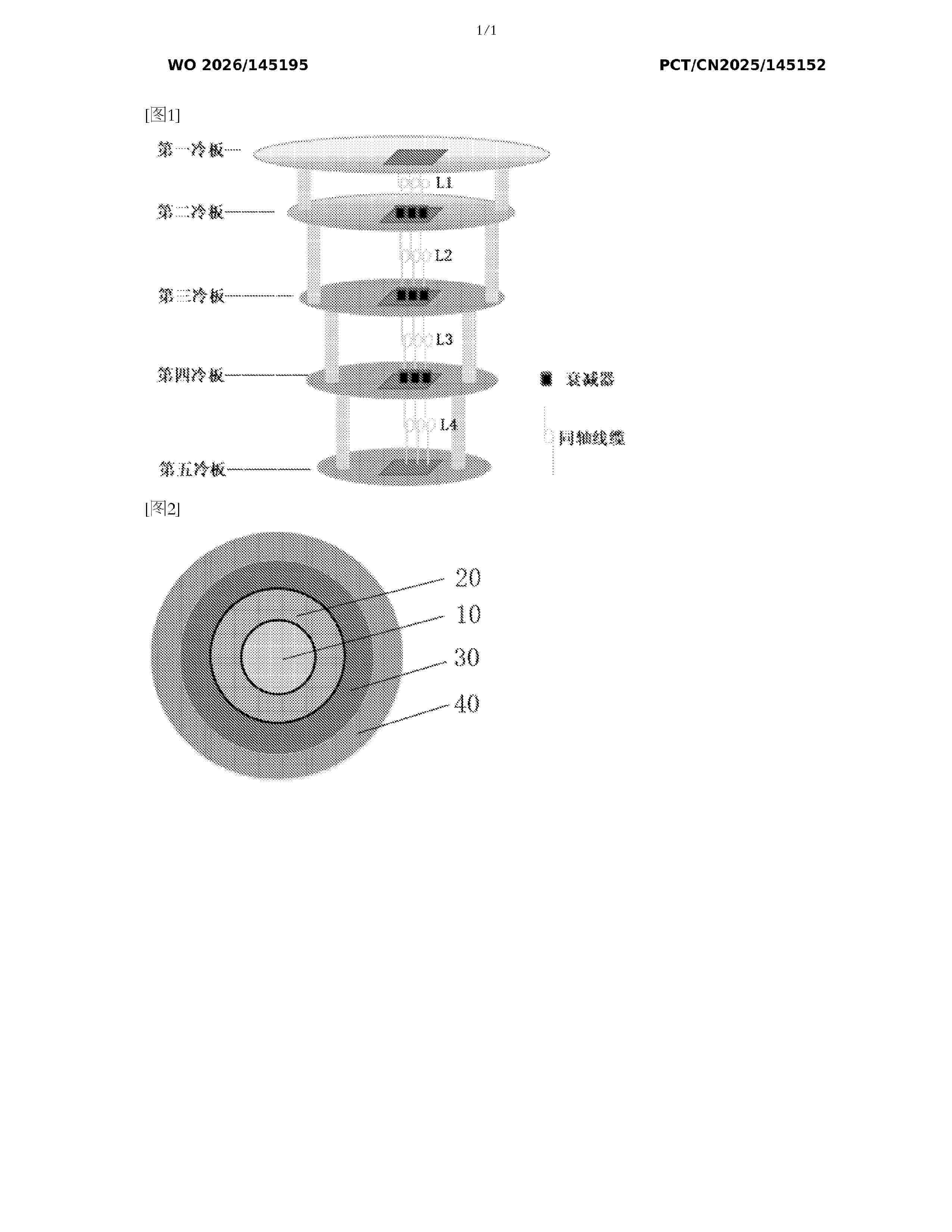
Resumen de: WO2026145195A1
Provided in the present invention are a superconductor-based coaxial cable of a dilution refrigerator, a dilution refrigerator, and a superconducting quantum computing device. The dilution refrigerator comprises at least a first temperature layer, a second temperature layer, a third temperature layer and a fourth temperature layer. The coaxial cable comprises a conductor layer, an insulating layer and a first shielding layer, the first shielding layer being arranged on the insulating layer at a first thickness. The coaxial cable further comprises a first coaxial cable segment disposed in the first temperature layer, a second coaxial cable segment disposed in the second temperature layer, a third coaxial cable segment disposed in the third temperature layer, and a fourth coaxial cable segment disposed in the fourth temperature layer, wherein the first thickness and the material of the parts of the first shielding layer at the first coaxial cable segment, the second coaxial cable segment, the third coaxial cable segment and the fourth coaxial cable segment are determined on the basis of a preset combination method.
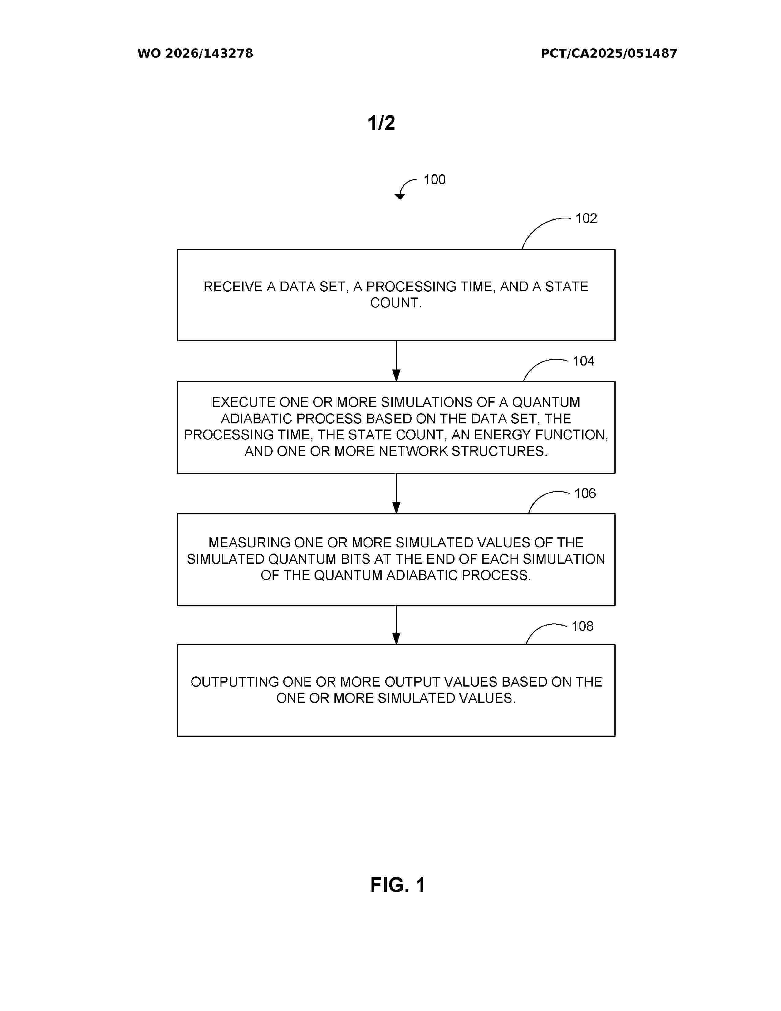
Resumen de: WO2026143278A1
Random number generation is crucial in applications such as cryptography, simulations, and statistical sampling. However, traditional methods often rely on algorithmic processes, which may not provide true randomness. An example solution may provide a computer-implemented method including: receiving a data set, a processing time, and a state count; executing one or more simulations of a quantum adiabatic process based on the data set, the processing time, the state count, an energy function, and one or more network structures, the one or more network structures including a representation of one or more initial simulated quantum bits; measuring one or more simulated values based on the one or more evolved simulated quantum bits at the end of each simulation; and outputting one or more output values based on the one or more simulated values, the one or more output values including one or more classical bit.
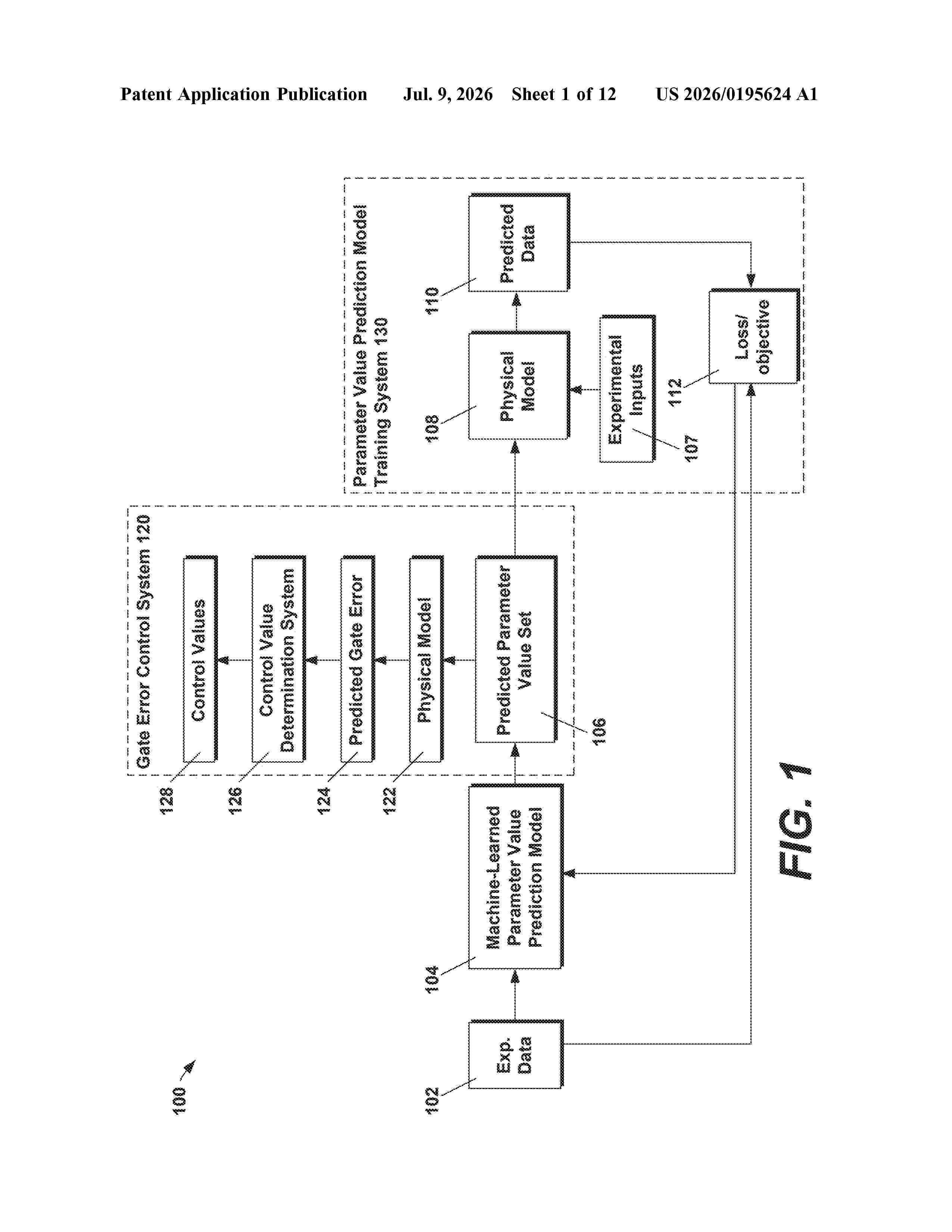
Resumen de: US20260195624A1
0000 The present disclosure provides systems and methods to measure quantum gate fidelity through swap spectroscopy. In particular, aspects of the present disclosure are directed to the derivation and use of a physical model that models non-Markovian quantum dynamics of interactions between one or more qubits of a quantum gate and one or more two-level-system (TLS) defects during operation of the quantum gate.
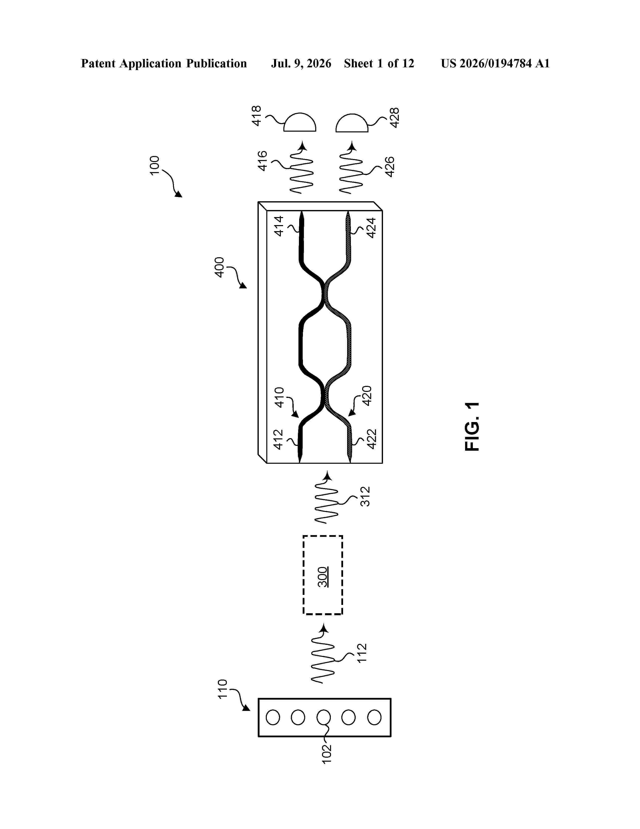
Resumen de: US20260194784A1
0000 A system includes a quantum source and an optical device coupled to the quantum source. The quantum source is configured to emit an entangled photon. The optical device is configured to route the entangled photon to one or more outputs. In some aspects, the optical device can include a photonic integrated circuit (PIC). Advantageously the system can provide a routing scheme to route (e.g., passively, actively, dynamically, or a combination thereof) entangled photons from one or more quantum sources (e.g., trapped ion, single-photon source, quantum emitter, etc.) between different nodes, a quantum frequency conversion scheme to match near-infrared photons (750 nm to 1260 nm) and/or telecommunication photons (1260 nm to 1675 nm) entangled with photons from one or more quantum sources to an operating wavelength of the optical device (e.g., PIC), programmable routing and entanglement distribution, and scalable long-distance quantum networks.
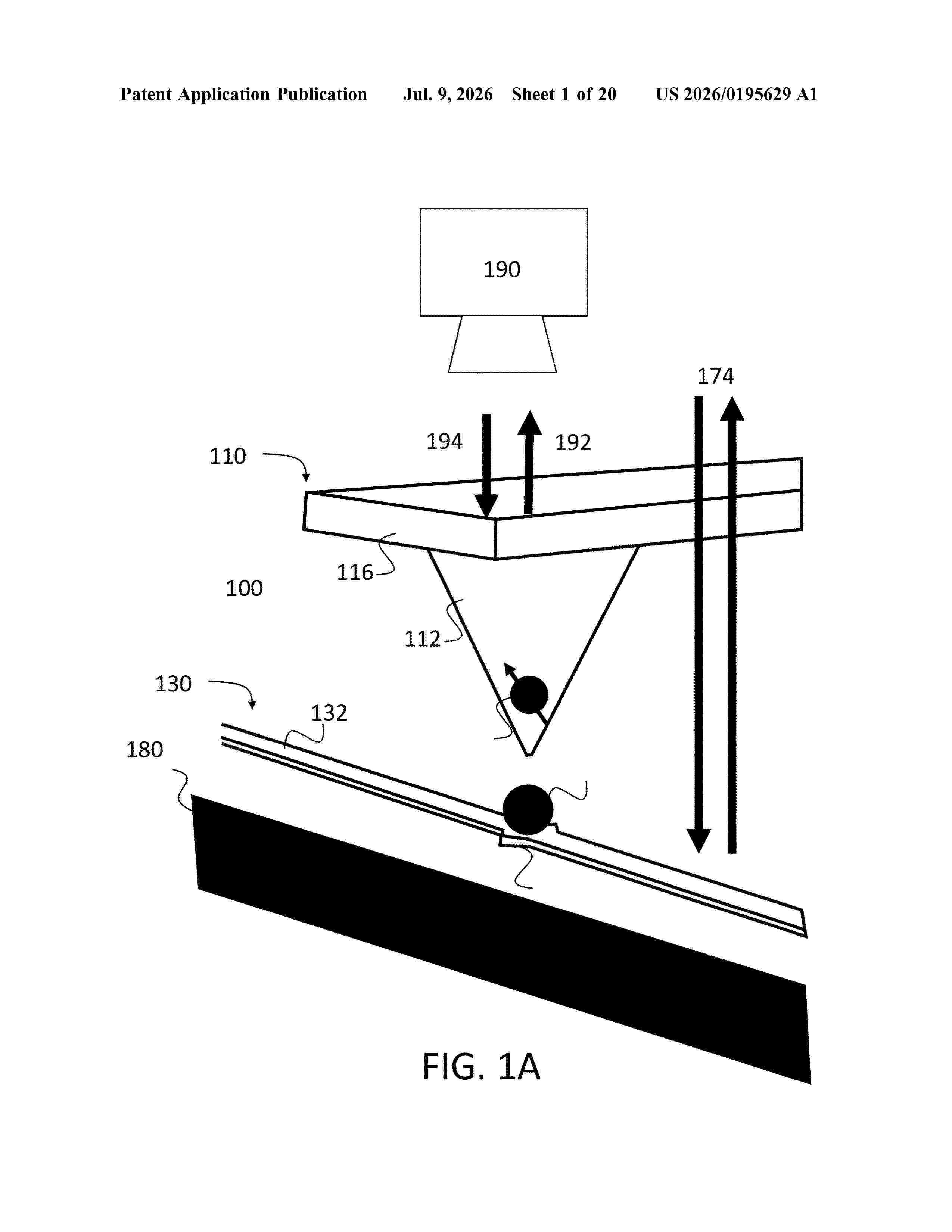
Resumen de: US20260195629A1
Systems and methods relate to mechanically mediated coupling of qubits to a mechanical resonator. Individual qubits can be coupled to a mechanical resonator, which can in turn couple to a second qubit that is separated from the first in distance, time, or both. Such mechanically mediated coupling can produce entangled qubit states over long distances and timescales. Arrays of qubits and/or mechanical resonators can be used to scale mechanically mediated coupling to larger numbers of qubits.
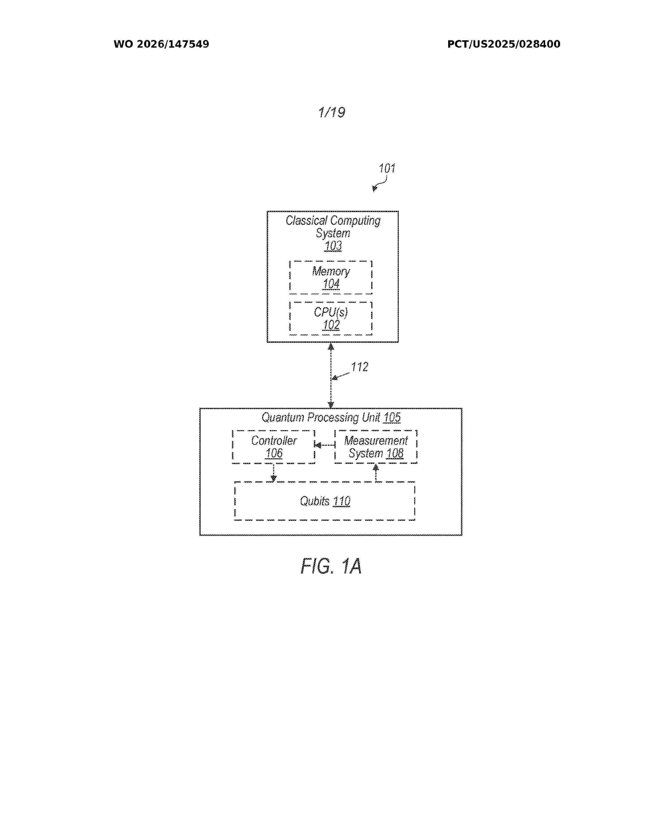
Resumen de: WO2026147549A2
Quantum computing devices, systems and methods for using quantum rejection sampling to prepare a quantum register in a target quantum state or to block encode a target matrix to operate on a quantum register. A preparation operator is applied to a first quantum register and a second quantum register to prepare the first quantum register in a reference state and to prepare the second quantum register in a uniform register state. The reference state approximates the target quantum state and is a summation over a set of computational basis states weighted by a reference function. Rejection sampling is performed on the first quantum register to prepare the first quantum register in the target quantum state.
Nº publicación: US20260195627A1 09/07/2026
Solicitante:
RUPAVATH RANA VEER SAMARA SIHMAN BHARATTEJ [US]
RUPAVATH Rana Veer Samara Sihman Bharattej
Resumen de: US20260195627A1
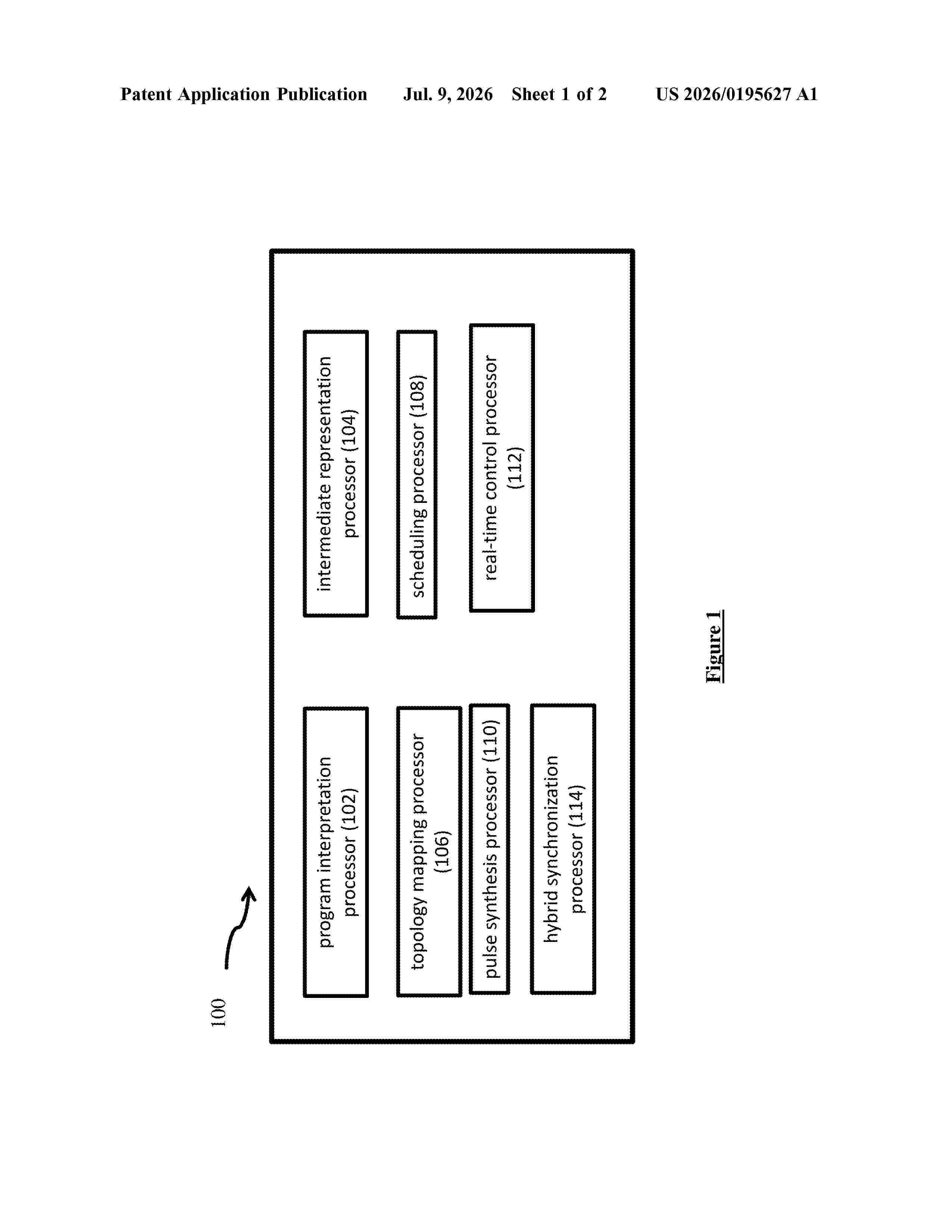
0000 The present invention relates to a system and method for quantum processing framework development comprising an integrated quantum processing control device configured to interface with at least one quantum processing unit. The system includes a program interpretation processor for converting high-level quantum technique definitions into an abstract syntax representation, an intermediate representation processor for generating a hardware-independent graph data structure, a topology mapping processor for mapping logical qubits onto physical qubits based on connectivity and calibration data, and a scheduling processor for optimizing execution order in view of coherence and fidelity parameters. A pulse synthesis processor generates time-domain waveform instructions corresponding to mapped quantum gate operations, and a real-time control processor transmits synchronized control signals to digital-to-analog conversion circuitry while acquiring measurement data through analog-to-digital conversion circuitry. A hybrid synchronization processor coordinates classical post-processing and conditional quantum operations within deterministic latency constraints.
 BOPI
BOPI
 Sede Electrónica