Si deseas distinguir tus productos, servicios o ambos de los de otra empresa, es posible que necesites una marca o nombre comercial. Descubre qué son, en qué consiste su procedimiento de registro y qué implica.

Información sobre los plazos de presentación de solicitudes de transformación de marcas de la Unión Europea en marca nacional española. Más información


Si tienes un nuevo dispositivo, producto o procedimiento que resuelva un problema técnico o tenga una ventaja práctica, existen distintas formas de protegerlo en España y en otros países. Descubre cómo hacerlo.

¿Tu innovación reside en la estética, la ornamentación o la apariencia de tu producto? Protégela mediante un diseño industrial. Descubre qué derechos confiere el registro y cómo realizar la tramitación.

Las indicaciones geográficas protegen el nombre de un producto originario de una zona geográfica, a la cual le debe una determinada calidad, reputación u otra característica. Descubre qué son, en qué consiste su procedimiento de registro y qué beneficios conceden.

Las patentes publicadas en todo el mundo son una valiosa fuente de información científica, técnica y comercial.

Si eres emprendedor/a o una empresa y quieres potenciar y mejorar la rentabilidad de tu negocio protegiendo de forma adecuada los activos intangibles de tu organización, en este espacio encontrarás lo necesario.


 153
resultados
153
resultados
 Última actualización
01/10/2026 [08:55:00]
Última actualización
01/10/2026 [08:55:00]


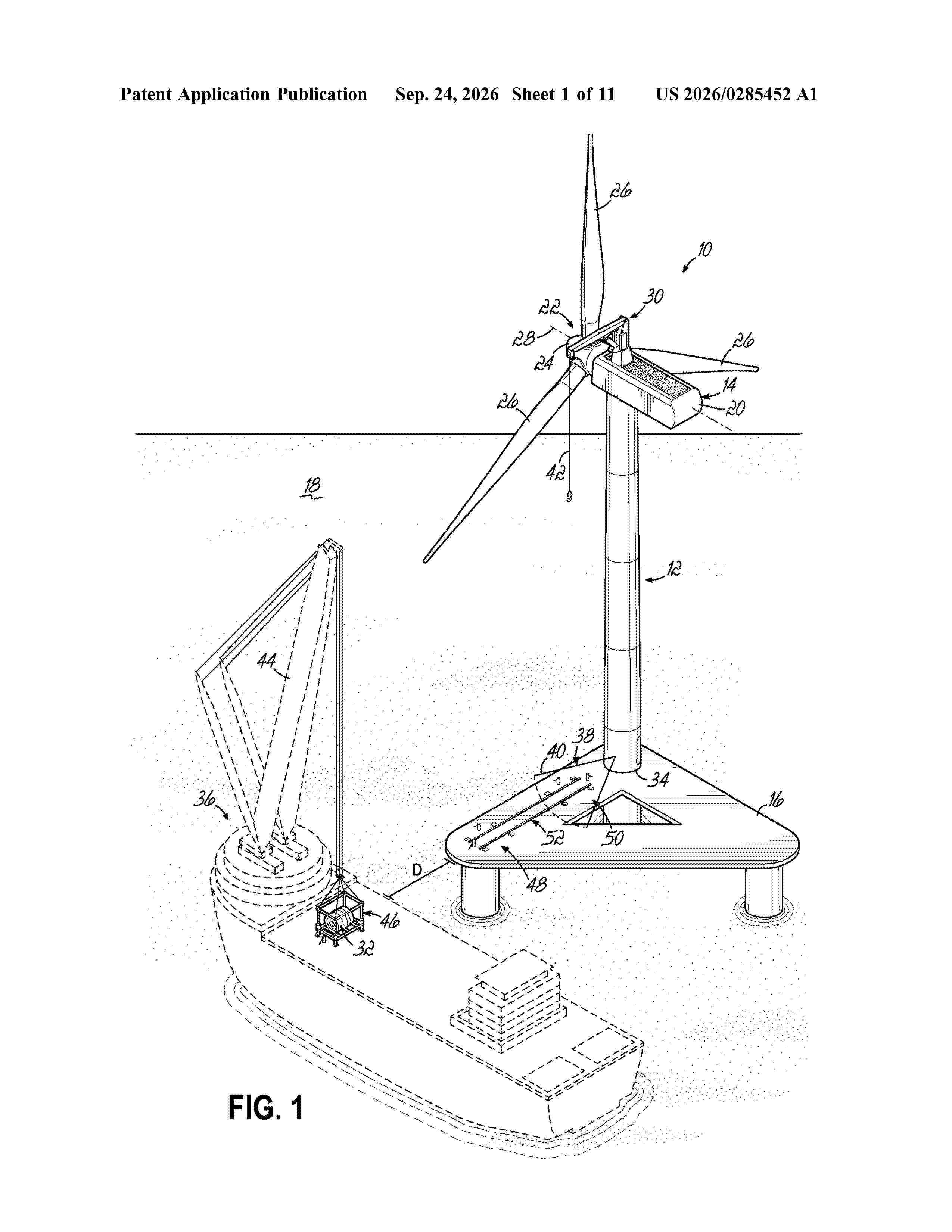
Resumen de: US20260285452A1
0000 A transportation skid (46) for transporting a wind turbine component (32) to a floating foundation (16) of an offshore wind turbine (10) is provided. The floating foundation (16) includes a tower interface (34) for attachment to an end of a wind turbine tower (12). The transportation skid (46) includes a skid frame (54) for supporting the wind turbine component (32) and a surface engagement element (56) configured to engage a component landing area (48) of the floating foundation (16). The component landing area (48) is spaced from the tower interface (34). The transportation skid (46) further includes a shock absorber (58) connecting the surface engagement element (56) and the skid frame (54) to soften the landing on the component landing area (48). A method of transporting the wind turbine component (32) to the floating foundation (16) of the offshore wind turbine (10) is also provided.

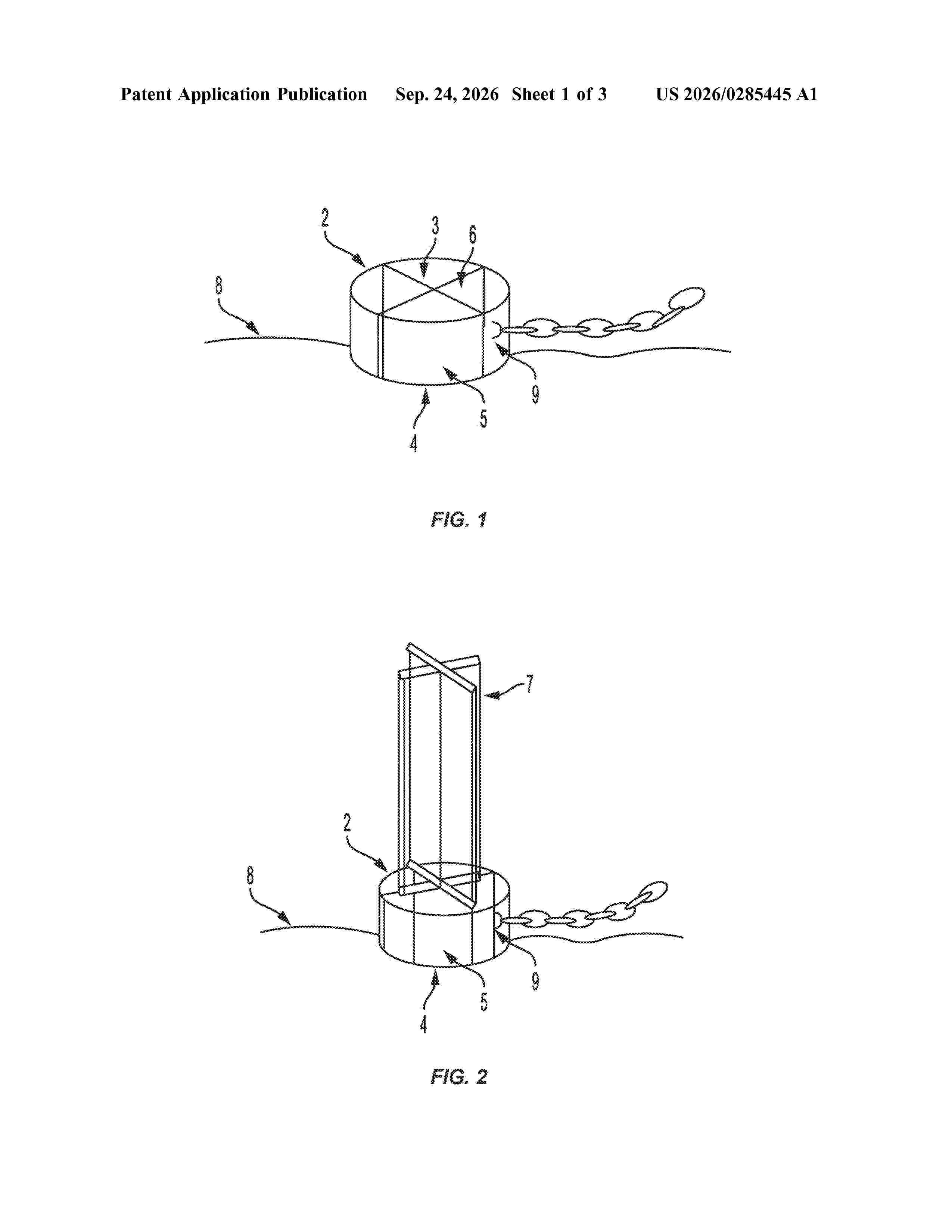
Resumen de: US20260285445A1
0000 Device for anchoring in a seabed comprising a hollow cylinder comprising an open upper base, an open lower base configured to be embedded in the seabed, a peripheral wall with an internal face and an external face, an internal stiffening structure attached to the internal face of the hollow cylinder and extending axially within the cylinder between the lower and upper bases of the cylinder, and an anchoring chain fastening means rigidly connected to the hollow cylinder.
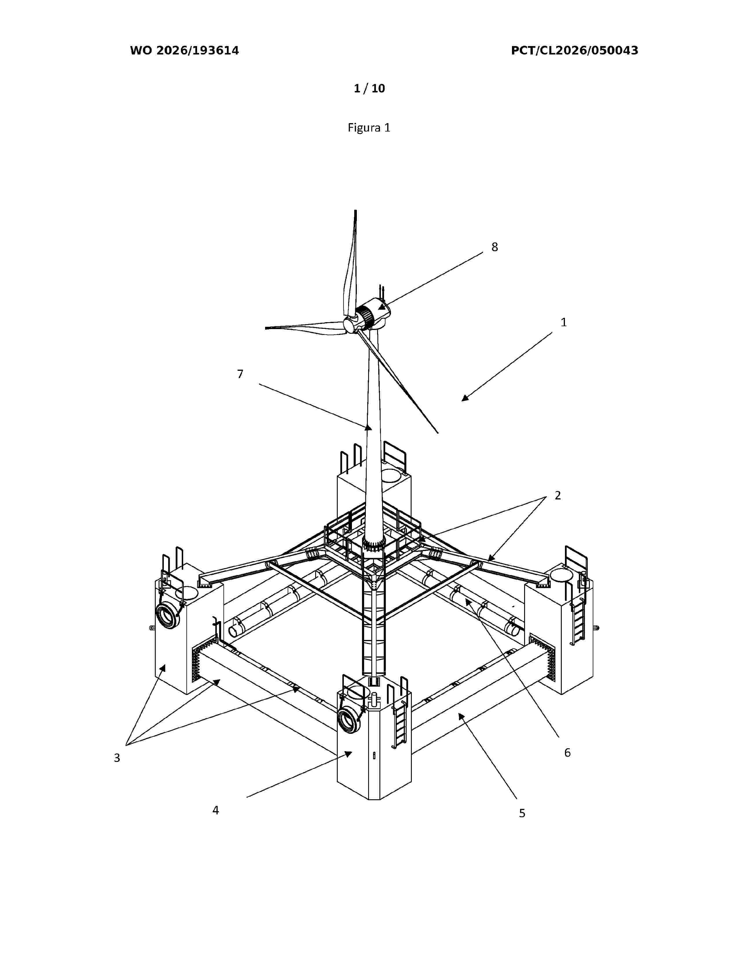
Resumen de: WO2026193614A1
The invention relates to a device for the generation and storage of modular floating wind energy (1) intended for the operation of floating wind power generation technologies in accordance with a damping and stability standard for heave, pitch and roll acceleration vectors, caused by the combined action of the wind on the wind turbine rotor and the waves on the flotation components, the modular construction of the components allows for standard workshop production, optimises the transportation of the components by lorry and assembly times on building berths and in shipyards, characterised by comprising at least one modular foundation for a wind turbine mast (2); at least one modular semi-submerged floating platform (3); and at least one mooring and anchoring system providing shock absorption and vertical ballast (46).
Resumen de: NL2036267B1
0001 A factory for producing an elongated tension member is provided. The factory comprises at least one apparatus for producing the elongated tension member. The at least one apparatus comprises: a feeder, a processing device and at least one end fitting device. The feeder is arranged to provide input material. The input material comprises: at least one load bearing yarn and/or at least one load bearing wire and/or load bearing fibres. The processing device is arranged to wind and/or twist and/or bundle the input material provided by the feeder. The at least one end fitting device is arranged to provide the elongated tension member with a proximal end fitting and a distal end fitting. The factory further comprises a buoyant body arranged to support said at least one apparatus for producing the elongated tension member. Fig. 1
Resumen de: WO2026189939A1
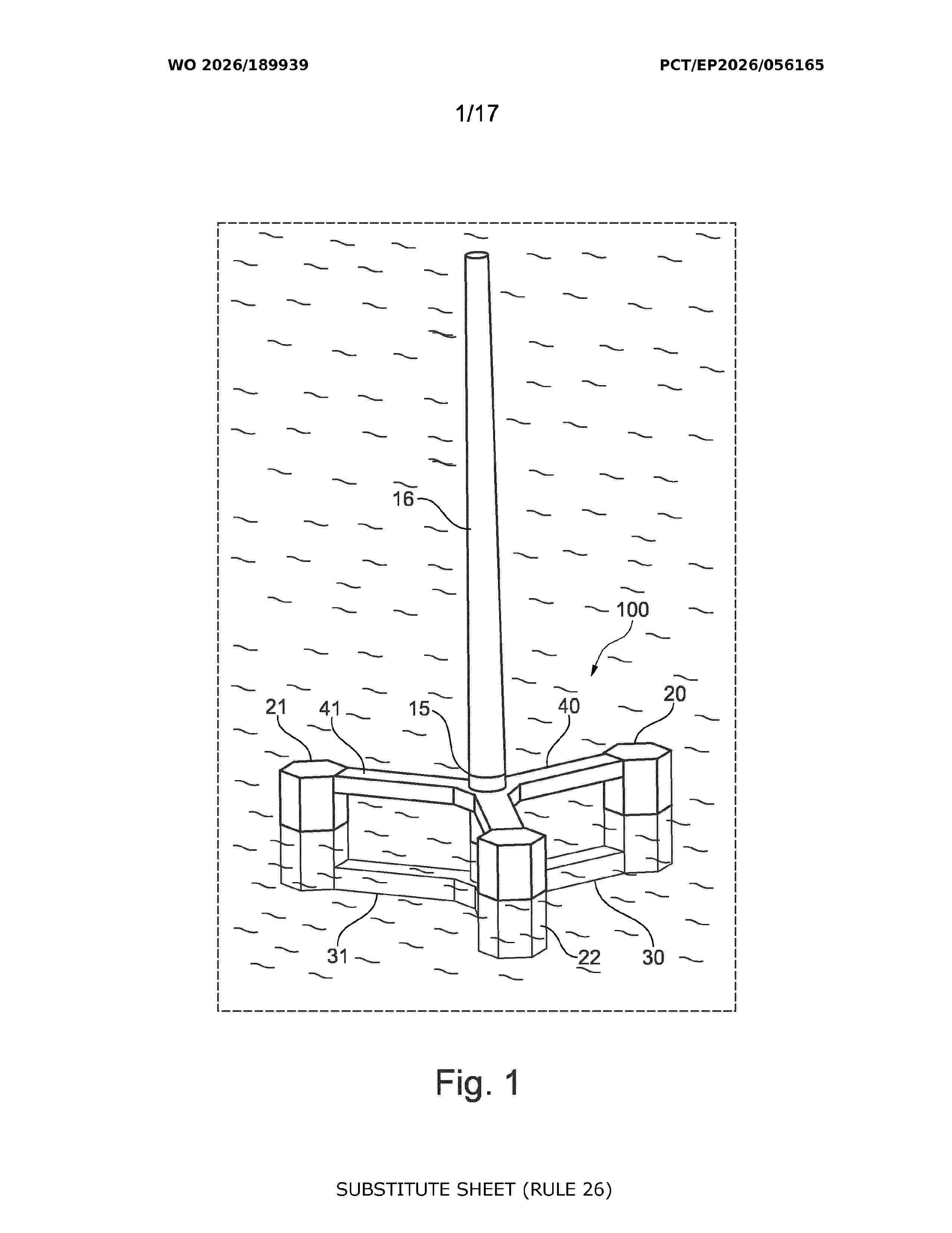
A floatable foundation (100) for a wind turbine generator, the floatable foundation (100) comprising: a frame section (140,141) formed by at least four structural plate parts (110-118), each structural plate part (110-118) having a shell plate (101) and a plurality of girders (103) welded to the shell plate (101); wherein each girder (103) has an apex bar (120) and a pair of leg bars (121,122) arranged between the apex bar (120) and the shell plate (101); and the frame section (140,141) comprises an internal box frame (133) fixed to girders (103) of each of the structural plate parts (110-118).
Resumen de: US20260274381A1
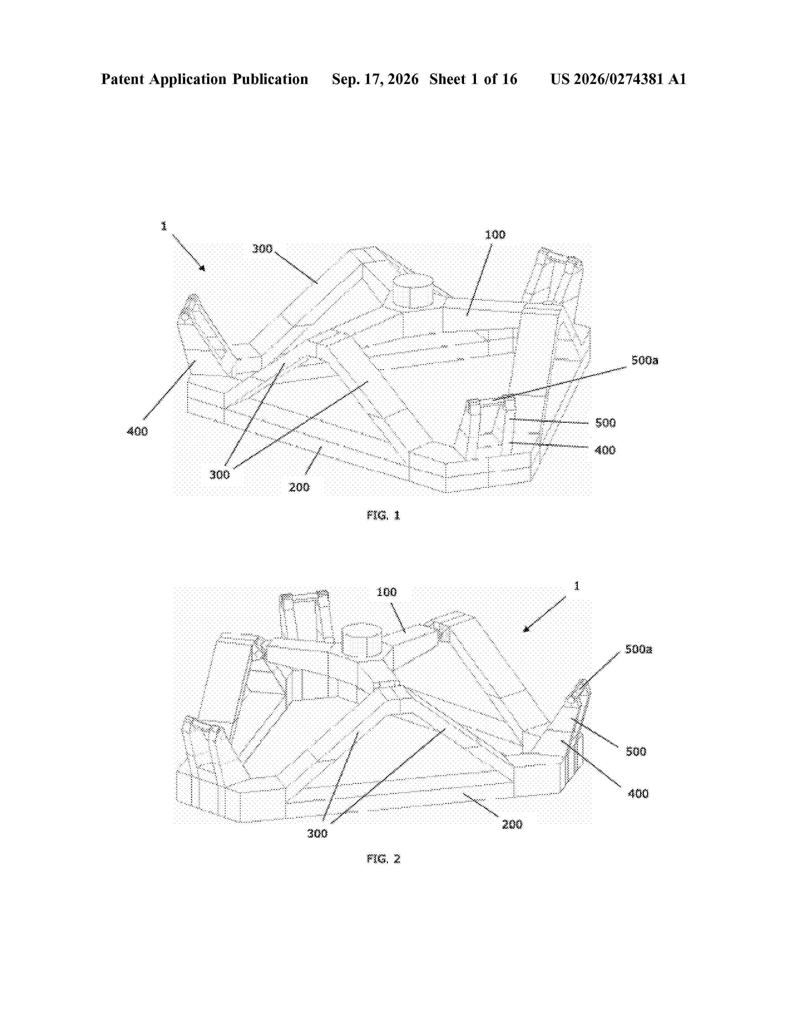
A floating platform includes a pedestal frame configured to serve as a support for a structure. The pedestal frame is attached to a bottom plate by means of a plurality of pillars such that, in operating condition, the pedestal frame is supported by the bottom plate by means of the pillars. The floating platform has a plurality of immersion floats projecting from the bottom plate to an intermediate distance between the bottom plate and the maximum height above the bottom plate of the pillars. It also includes a geometry that allows the platform to be manufactured exclusively with flat panels.
Resumen de: EP4552966A1
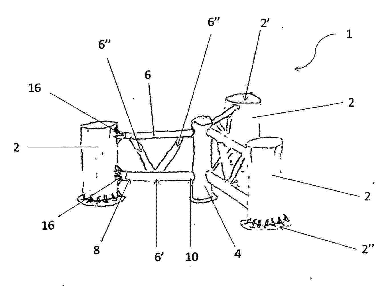
0001 The invention relates to an offshore wind turbine platform (1) comprising: - a main body (4) intended to receive a mast of a wind turbine attached to it, - several floats (2), each float comprising an upper metal wall (2') forming an upper end of the float, a lower metal wall (2") forming a lower end of the float, and several side walls (18, 28, 28', 48, 58) connecting the upper and lower metal walls to create a watertight enclosure of the float, - several metal connection structures (6), each metal connection structures comprising at least a first end (8) attached to one float and a second end (10) attached to the main body.
Resumen de: EP4806578A1
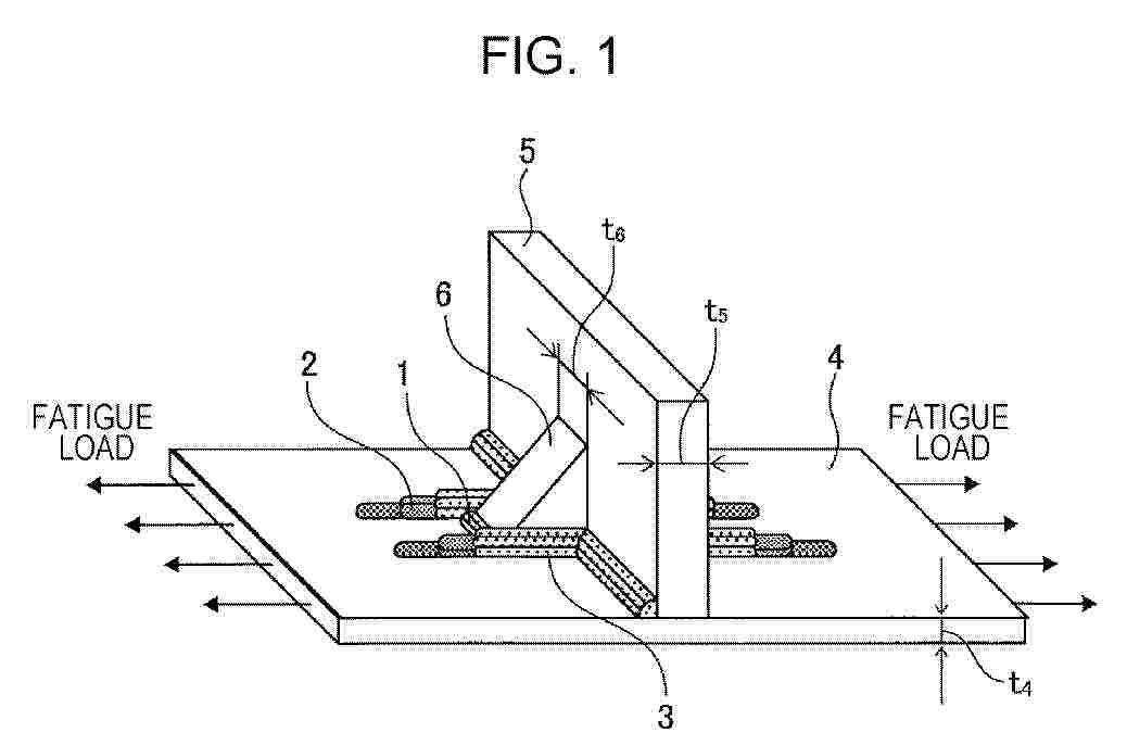
Provided a multi-layer welding method and a multi-layer welded joint in a large structure such as a floating offshore wind power generation facility. The present invention is a multi-layer welding method in which a bracket 6 for reinforcing a vertical plate 5 provided on a steel plate 4 is welded to the steel plate 4 and the vertical plate 5, the welding method including: forming a first weld bead 1 in multiple layers along a short side of a rectangular contact surface 6a at which the bracket 6 is in contact with the steel plate 4; and subsequently forming a second weld bead 2 and a third weld bead 3 in multiple layers such that the second weld bead 2 and the third weld bead 3 are provided along long sides of the rectangular contact surface 6a, overlap end portions of the first weld bead 1, and further extend onto the steel plate 4.
Resumen de: EP4806778A1
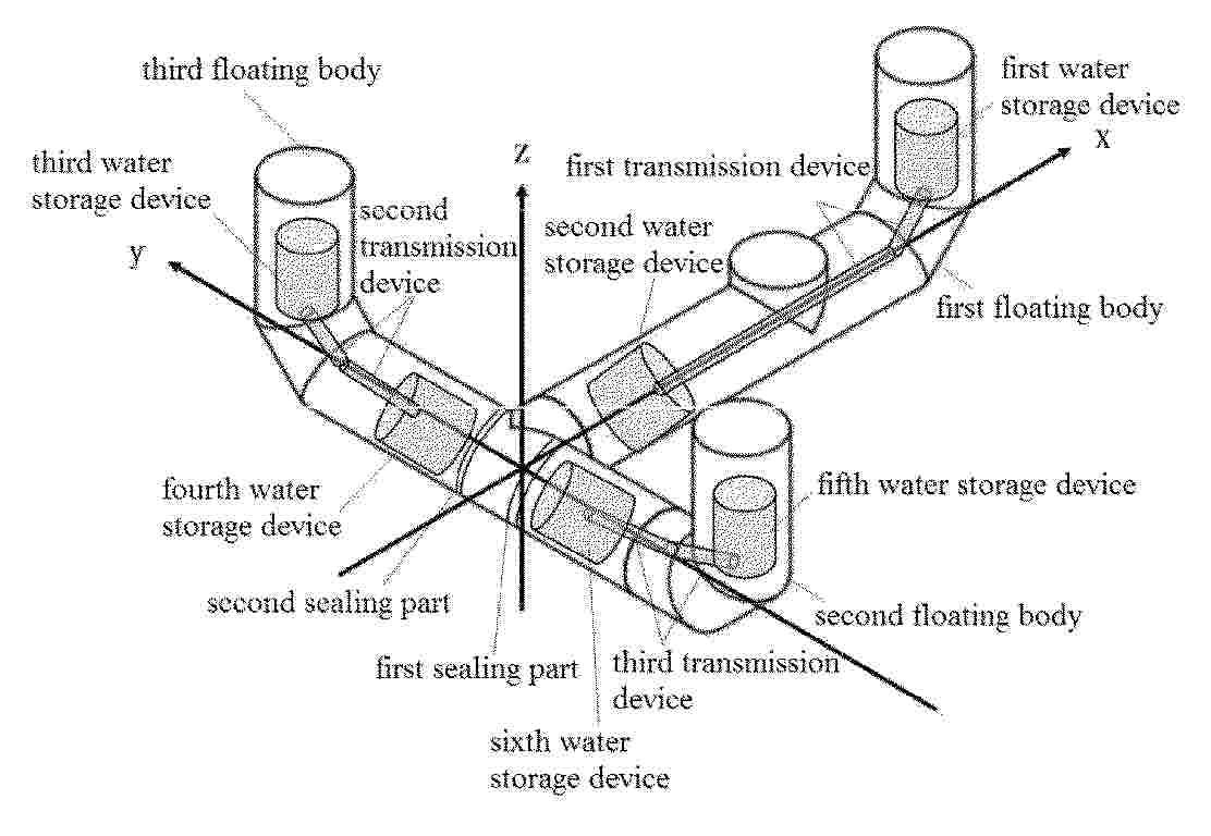
0001 A floating wind power floating body and a method for balancing the floating wind power floating body are provided. The first floating body is connected with the second floating body through a first sealing part; the first floating body is connected with the third floating body through a second sealing part. The first water storage device is connected with the second water storage device through first transmission devices; the third water storage device is connected with the fourth water storage device through second transmission devices; the fifth water storage device is connected with the sixth water storage device through third transmission devices.
Resumen de: WO2026186047A1
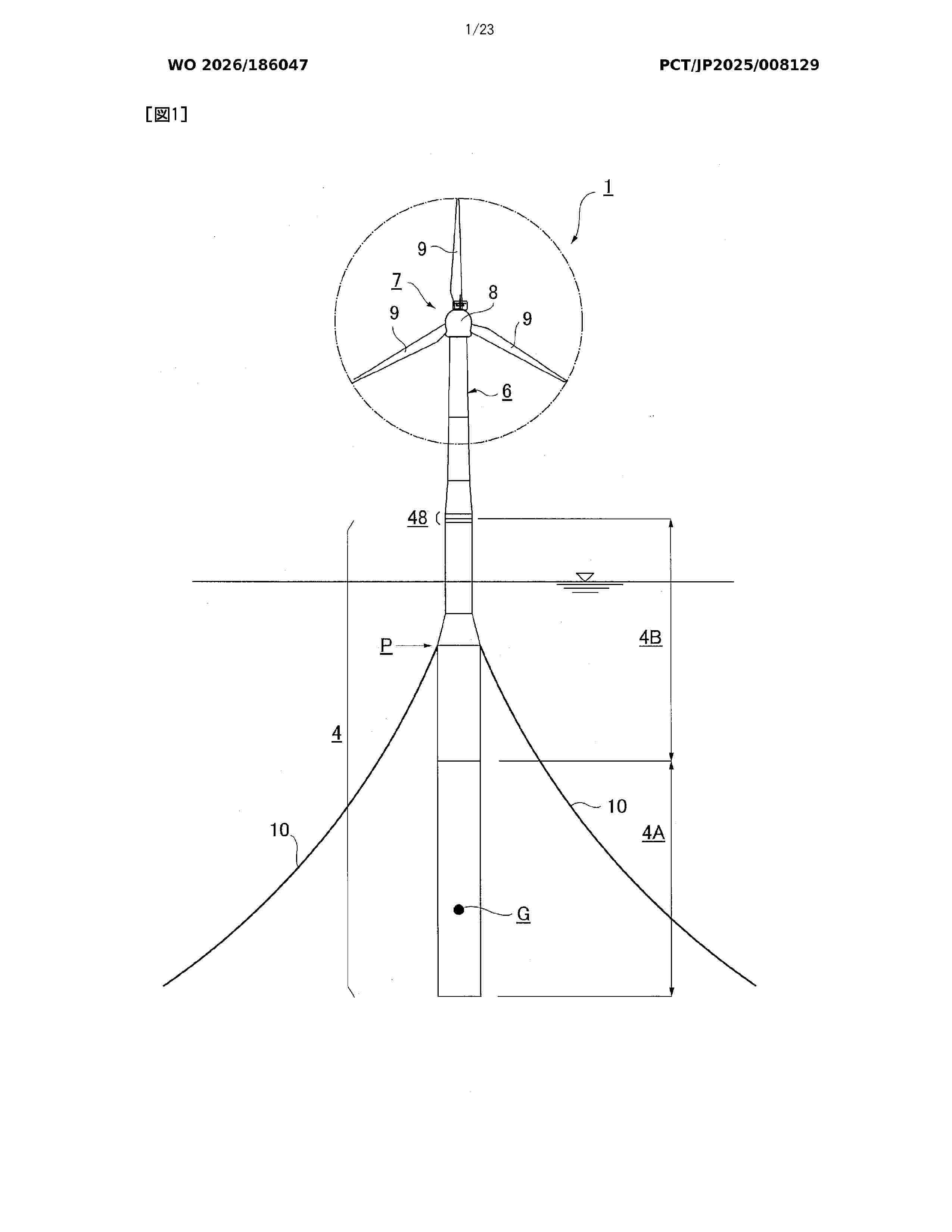
Problem To provide a connection device capable of stably and efficiently connecting a superstructure to a floating body. Solution A connection device 48 comprises a floating body-side connection device 49 provided at an upper end of a floating body 4, and a tower-side connection device 50 provided at a lower end of a tower 6. The floating body-side connection device 49 has at least two introduction pipes 54, 55, and the tower-side connection device 50 has a plurality of introduction pins 59, 60 provided corresponding to the introduction pipes 54, 55. The introduction pipes 54, 55 comprise engagement pipe portions 54A, 55B having through holes formed therein, and guide portions 54B, 55B, and the introduction pins 59, 60 have a cross-section that allows insertion into the through holes of the engagement pipe portions 54A, 55B, and are held so as to be slidable in an upward direction. With the corresponding introduction pipes 54, 55 and introduction pins 59, 60 respectively fitted together, a connecting flange 53 of the floating body-side connection device 49 and a connecting flange 58 of the tower-side connection device 50 are fastened together by bolt-and-nut members 65, 65.
Resumen de: WO2026186125A1
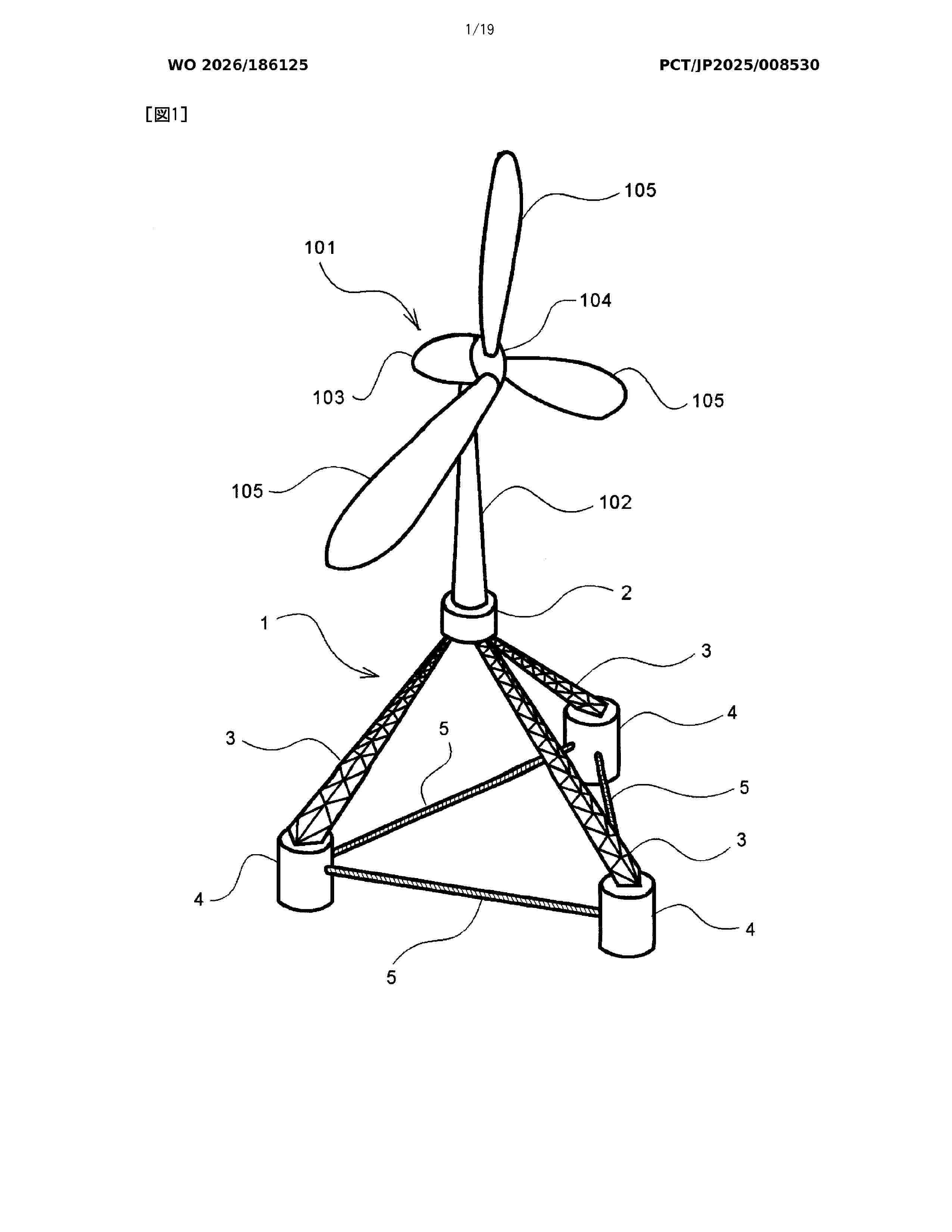
The present invention addresses the problem of providing a floating body structure, and the problem is solved by a floating body structure 1 characterized by comprising a facility holding body 2 that holds an offshore facility 101, three or more inclined leg members 3 each having an upper end connected to the facility holding body 2 and a lower end swingable in directions in which the lower ends move toward and away from each other, floating bodies 4 attached to the lower ends of the inclined leg members 3, and a wire 5 that limits the distance between the floating bodies 4, wherein: in a state in which the lower ends of the inclined leg members 3 are directed obliquely downward around the facility holding body 2, the floating body structure 1 floats on the sea by buoyancy generated in the floating bodies 4; and tension is generated in the wire 5 by gravity acting on the offshore facility 101 and the facility holding body 2, and the distance between the floating bodies 4 is maintained constant.
Resumen de: GB2635162A
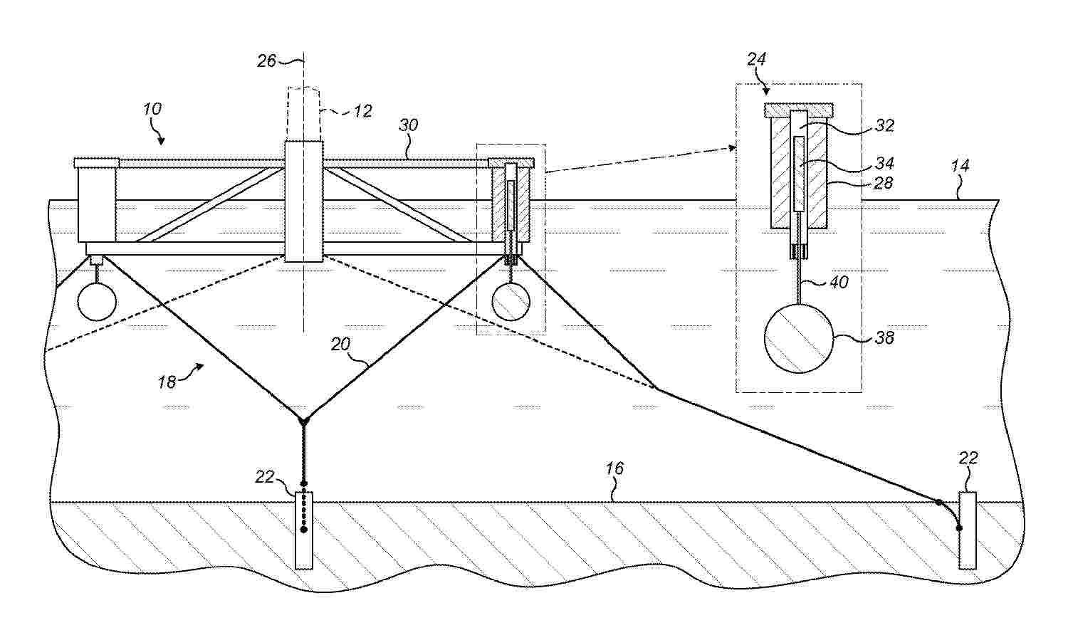
Motion of a floating body 10 is damped by anchoring a piston 34 with a sea anchor 38 to restrict movement of the piston, permitting greater movement of a chamber 32 that surrounds the piston and is fixed to the body, but braking the resulting relative movement between the chamber and the piston by displacement of fluid in the chamber. Thus, a motion damper 24 has a brake structure that comprises a submerged sea anchor suspended in a water column and connected to a piston. The piston is movable within an elongate chamber that is in fixed relation to the floating body and that contains a fluid such as water. The sea anchor is connected to the piston by means of a link 40.
Resumen de: WO2025095785A1
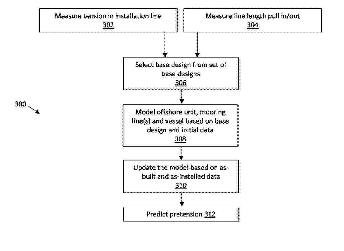
A computer-implemented method of achieving a target pretension in one or more mooring lines of a physical floating offshore unit, the method comprising: measuring a tension in an installation line configured to install the physical floating offshore unit, measuring a line length pull in/out of the installation line; generating a model comprising a digital representation of the physical floating offshore unit's physical properties and/or physical behaviours, wherein the physical floating offshore unit comprises one or more mooring lines and wherein the model is configured to model the one or more mooring lines, the model further comprising a digital representation of physical properties and/or physical behaviours of an installation vessel that is configured to install the physical floating offshore unit, wherein generating the model comprises selecting a base design for the model from a set of base designs based on the measured tension and measured line length pull in/out and modelling the physical floating offshore unit's physical properties and/or physical behaviours based on initial data, wherein the initial data is to be updated based on as-built and as- installed data comprising (i) operations data specific to the physical floating offshore unit and the mooring lines and (ii) marine execution data, and estimating, by the model, based on the as-built and as-installed data, a predicted pretension in the one or more physical mooring lines such that vessel disconnection from
Resumen de: EP4803740A1
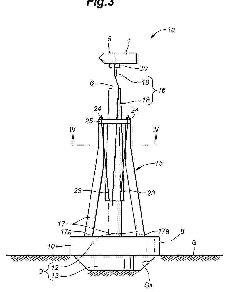
An object of the present invention is to provide a construction method for a floating wind power generation facility which is less susceptible to wind and waves when towing. A provisional assembly (1a) is assembled on land. The provisional assembly (1a) includes a base part (8) of a floating body (2) and a provisionally mounted member (6, 13, 16) disposed at a position different from a position at completion. After assembly of the provisional assembly (1a), the provisional assembly (1a) is launched. After being launched, the floating wind power generation facility under construction is towed to its installation position, and the provisionally mounted member (6, 13, 16) is disposed at the position at completion. Since the provisional assembly (1a) is shorter in length in the up-down direction than the completed floating wind power generation facility, the provisional assembly (1a) is less susceptible to wind and waves when towed.
Resumen de: US20260257776A1
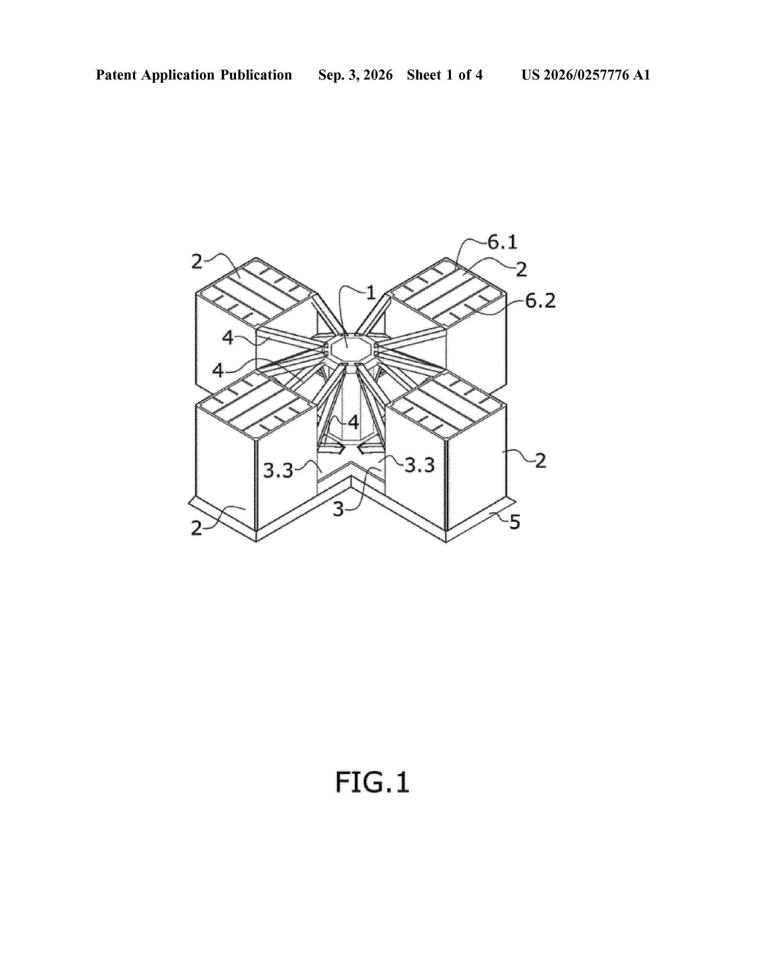
The present invention relates to a floating concrete structure for offshore wind applications, comprising a semi-submersible platform which in turn comprises: an inner column (1), a plurality of outer columns (2) distributed around the inner column (1) equidistant thereto (1), wherein the inner column (1) or one of the outer columns (2) supports a wind turbine tower, a plurality of beams (4) connecting each outer column (2) with the inner column (1). The floating structure further comprises a pontoon (3), the inner column (1) and the plurality of outer columns (2) being supported on the pontoon (3) and the plurality of beams (4) comprises first beams (4.1) which extend parallel to the pontoon (3) between the upper end of the inner column (1) to a point of attachment with the outer columns (2).
Resumen de: US20260258787A1
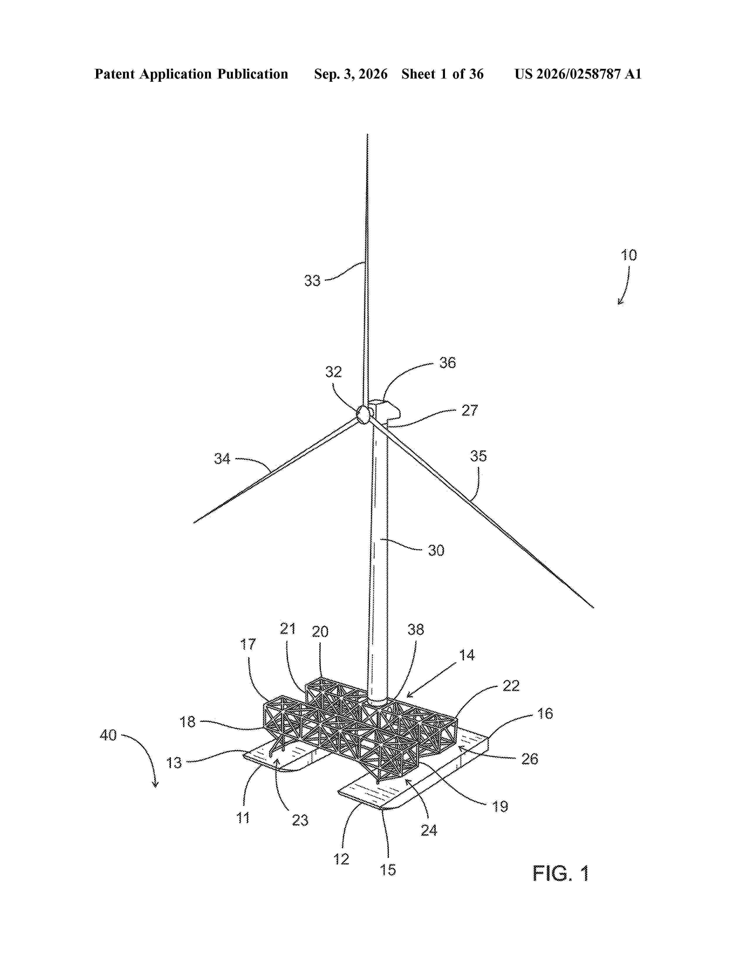
0000 An offshore floating wind turbine apparatus provides a pair of spaced apart hull sections with a space between the hull sections. One or more gantries each connect to the hull sections. The one or more gantries are spaced apart and connected to the hull sections with pivotal or universal joint connections. A wind turbine tower has upper and lower end portions. The wind turbine tower has a lower end portion with a base that is mounted to one of the gantries. The tower upper end portion has a rotor, hub, nacelle, and blades. A mooring system preferably holds the hull sections on a desired offshore marine location.
Resumen de: US20260258786A1
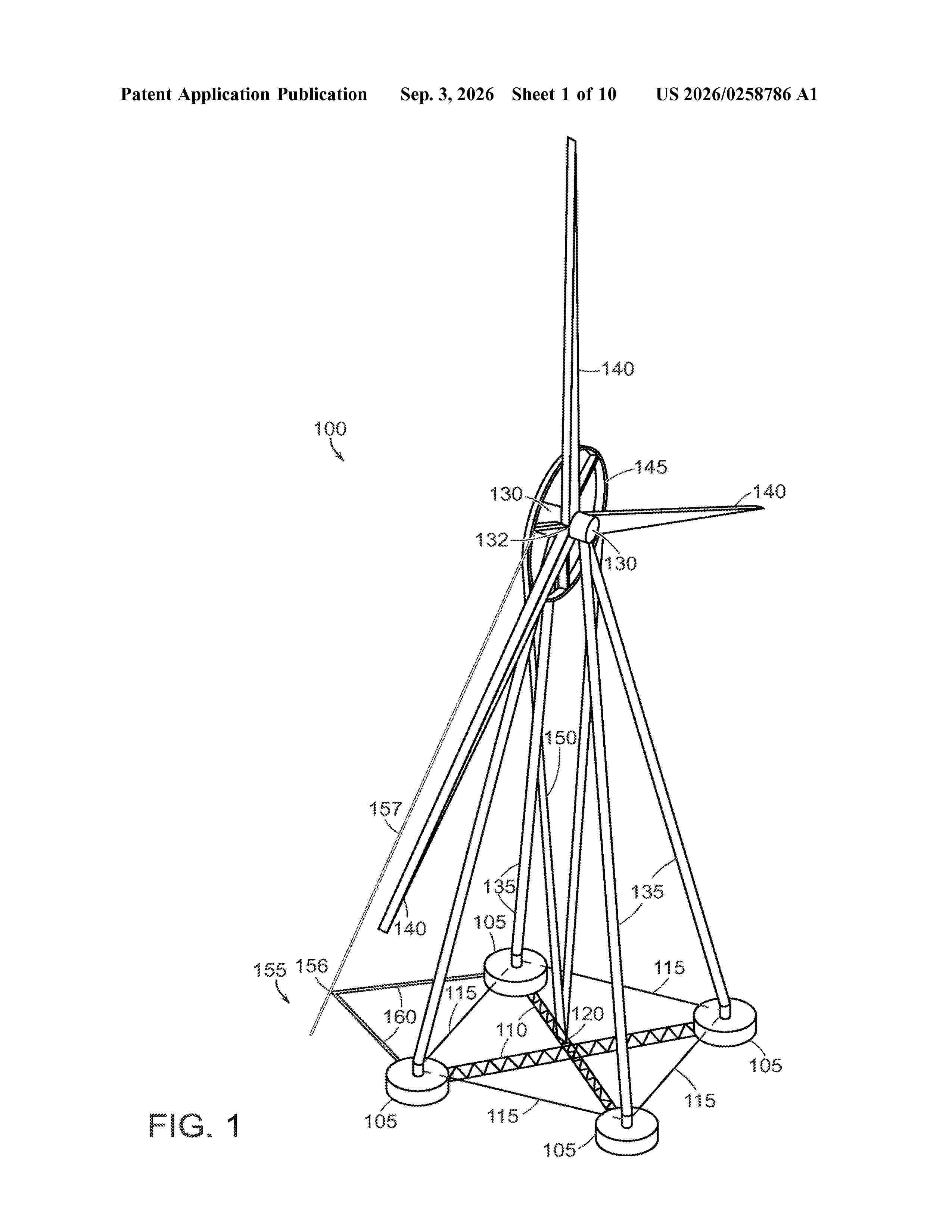
A high capacity, shallow draft, ocean-borne wind turbine is described, featuring a floating structure with at least three floats and a turbine rotor coupled to a generator with a power capacity of at least 3 MW. The turbine includes multiple blades, each with a length, and an operational draft less than about one-sixth of the blade length. Variations include configurations with round surf ace piercing floats and specific arrangements of four floats in a square formation. The design ensures a draft in operation of less than 1 meter per MW of rated capacity, providing an efficient and stable platform for offshore wind energy generation.
Resumen de: US20260258788A1
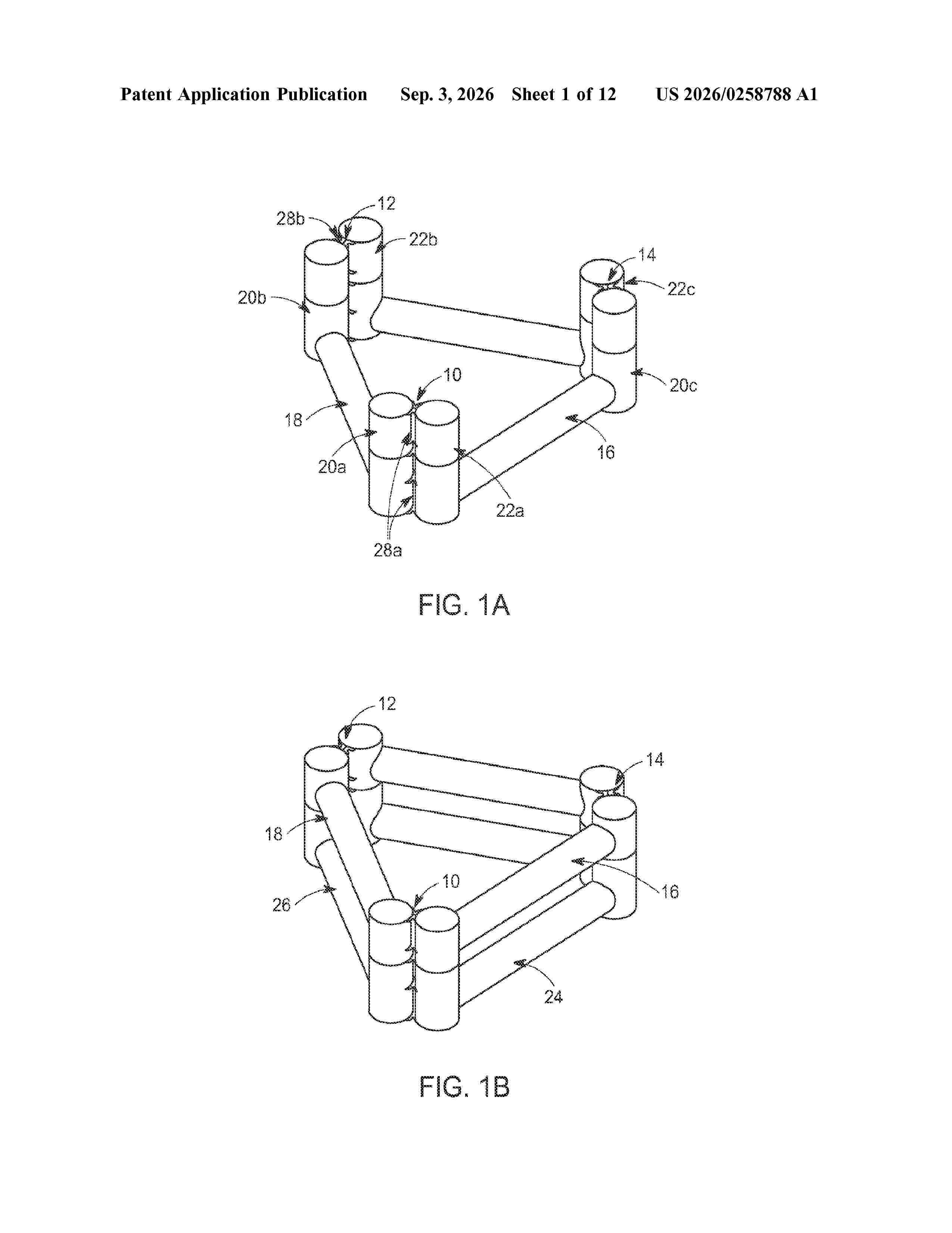
0000 Delivery of a high volume of floating systems for wind turbines can involve the standard design of sections, such as “tubes” or “cans,” comprising a rolled plate and ring stiffeners. The delivery can then involve the transportation of the sections in blocks to an assembly site that is closer to the planned installation point. The sections are used to manufacture semi-submersibles at the assembly site using a barge with cranes. The delivery can then involve the transportation of each of the semi-submersibles to a platform, such as a standard jack-up vessel or a crane jacket, near which the semi-submersible is temporarily attached to allow the installation of the Tower, the nacelle, and blades. Finally, the delivery involves the transportation of the completed wind turbine to the planned installation point, where it can be attached to a pile driven into the seafloor or moored during use. 0000 WO
Resumen de: US20260257770A1
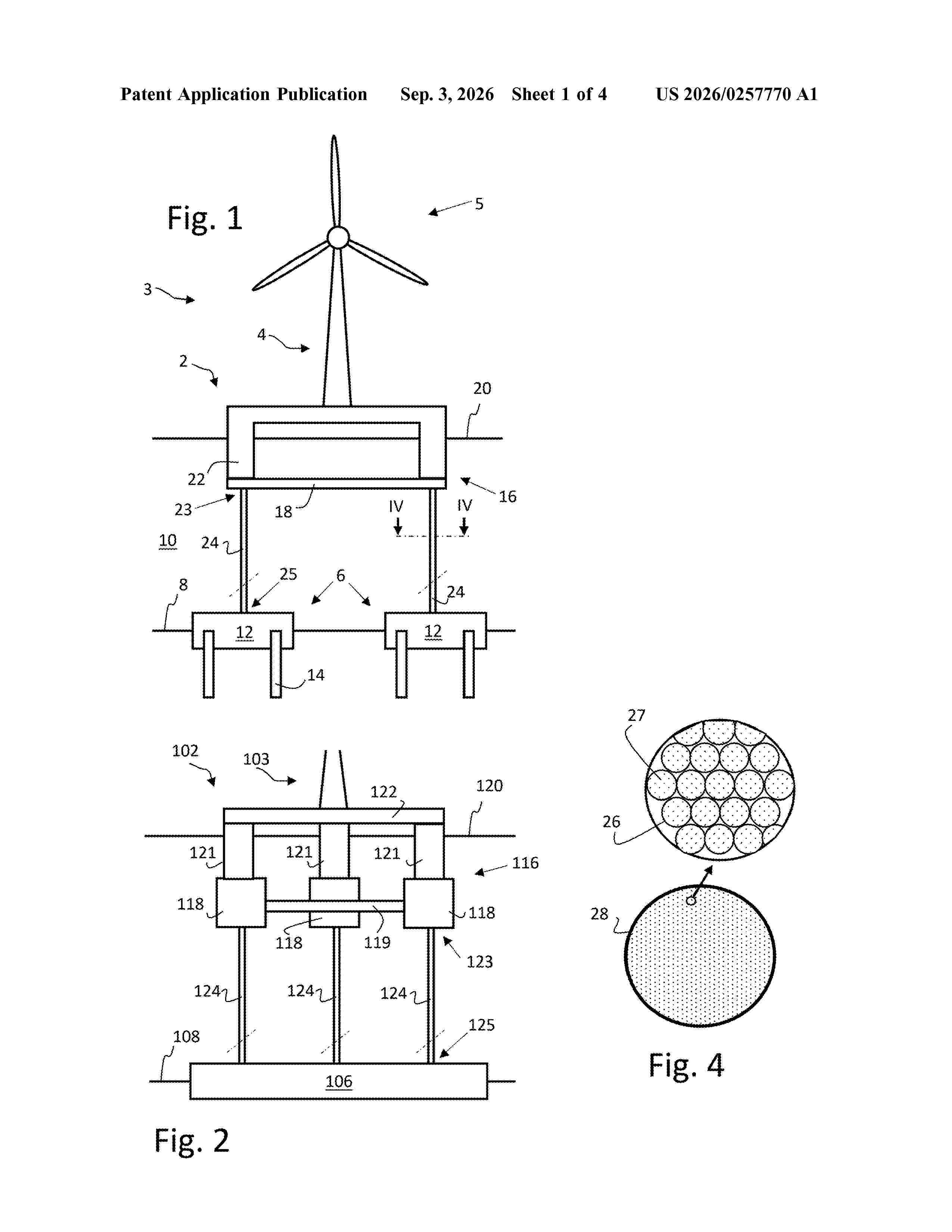
A tendon (224) for a tension leg platform (202), TLP, is provided. The TLP has a foundation (206), connectable to a bottom (208) of a body of water, and a buoyant hull (216). The tendon has a length of at least 300 meters, a proximal end (223), and a distal end (225). The tendon also has a proximal end fitting at the proximal end and a distal end fitting at the distal end. The tendon is connectable with the proximal end fitting to the hull and with the distal end fitting to the foundation to provide a pulling force on the hull. The tendon is formed with basalt fibres for transferring the pulling force from the proximal end fitting to the distal end fitting.
Resumen de: US20260257775A1
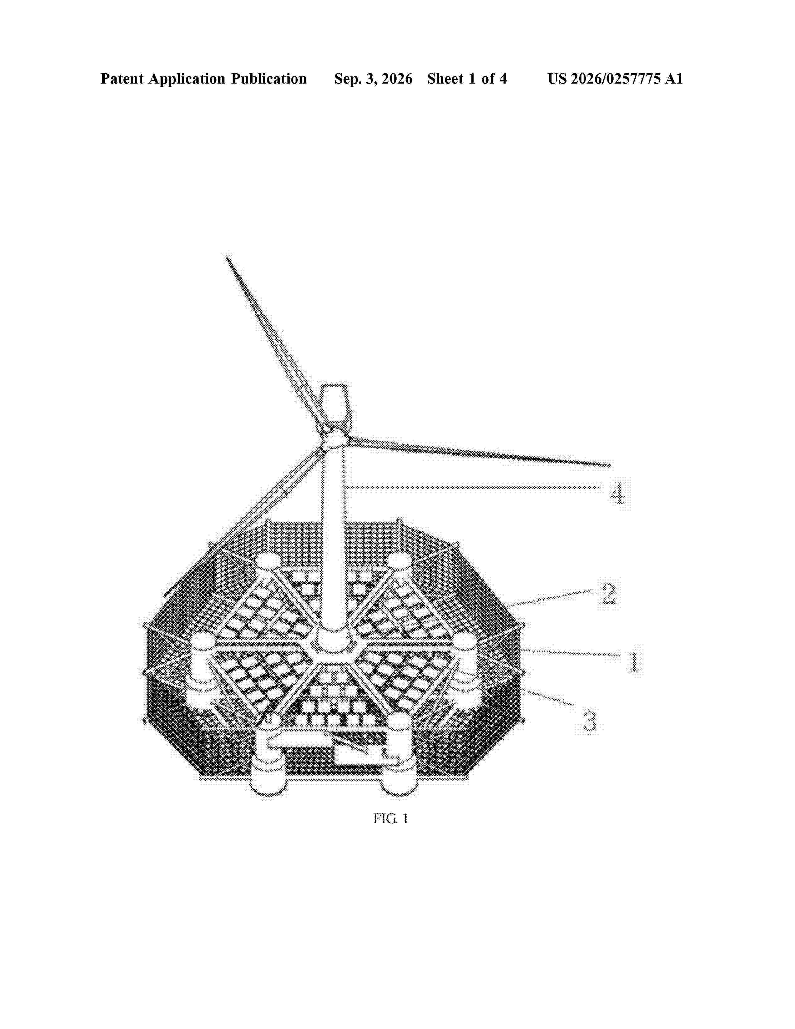
0000 A multifunctional integrated platform, includes a wind turbine, a photovoltaic power generation system, a floating body, and a net cage. The wind turbine, the photovoltaic power generation system and the net cage are all mounted on the floating body. The wind turbine is configured to perform wind power generation, and the photovoltaic power generation system is configured to perform photovoltaic power generation.
Resumen de: EP4800240A1
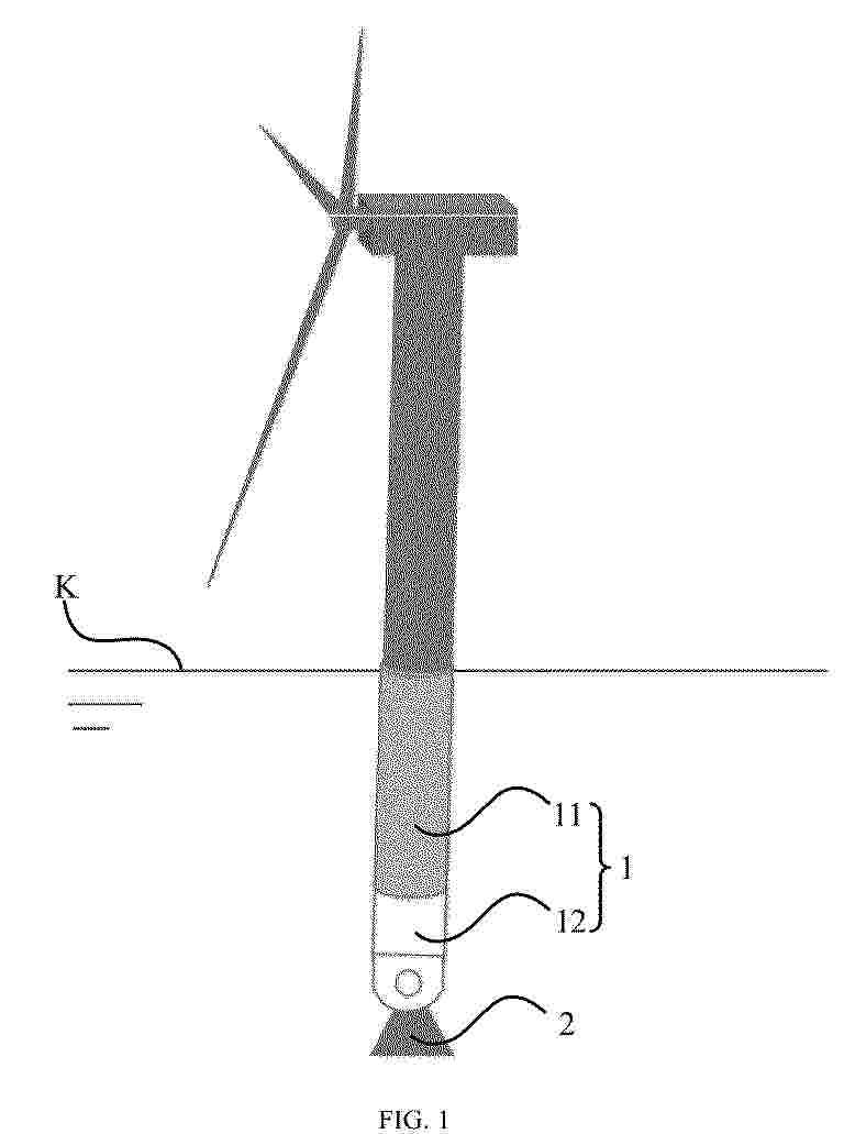
The present invention belongs to the technical field of offshore power generation, and specifically discloses a universal-joint-type connection device for connecting an offshore wind turbine platform to the seabed. By installing a cross universal-joint-type connection structure at the bottom of the main body of a tension-type floating offshore wind turbine platform and using the cross universal-joint-type connection structure as the swing center, when encountering strong winds or waves, the platform can swing in response to the winds or waves and float under the action of buoyancy. Meanwhile, by connecting the floating platform to the seabed, the forces acting on the platform main body can be transmitted to the seabed through the universal joint, avoiding the torsion phenomenon that occurs when mooring cables are used, improving the connection stability between the platform main body and the seabed, providing effective support for wind power generation equipment, and enabling the wind turbine unit to maintain stable wind-facing operation.
Resumen de: EP4799917A1
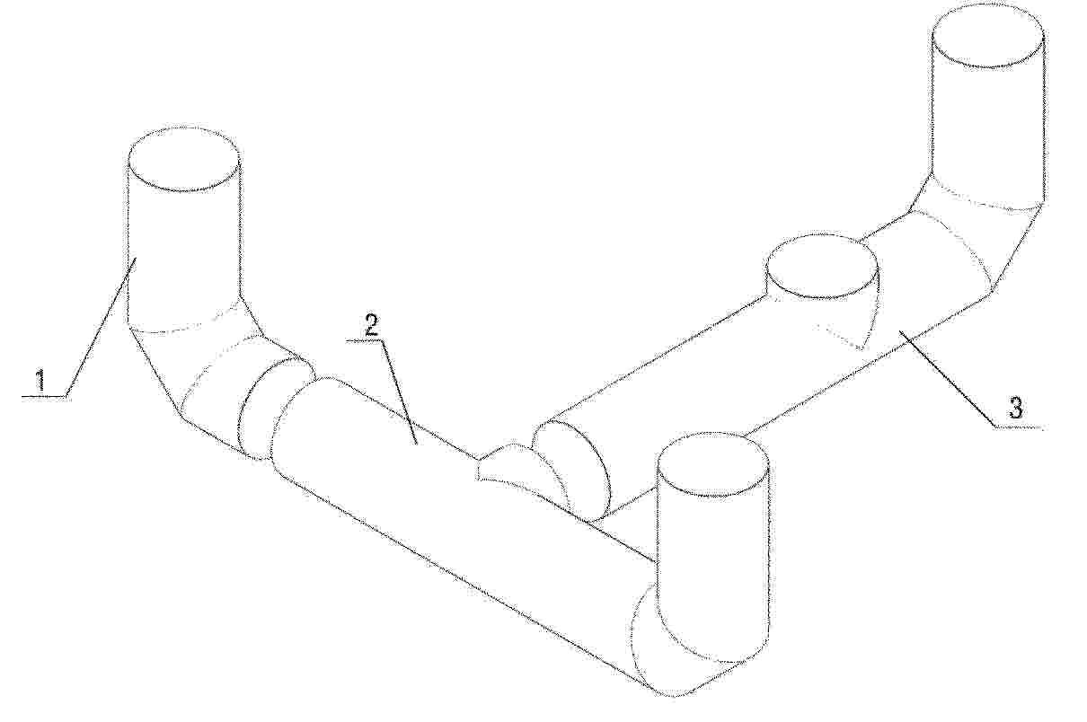
A floating foundation is provided and includes a plurality of foundation modules. The plurality of foundation modules are spliced and connected, and the foundation modules at least include a first foundation module extending in a first direction, a second foundation module extending in a second direction and a third foundation module extending in a third direction after the plurality of foundation modules being spliced, where the second foundation module and the third foundation module are located in a same plane, and a plane of the first foundation module is higher than planes of the second foundation module and the third foundation module being located. The first direction, the second direction and the third direction form a three-dimensional coordinate system. In addition, the disclosure also provides a method for assembling the floating fan.
Resumen de: US2025137431A1
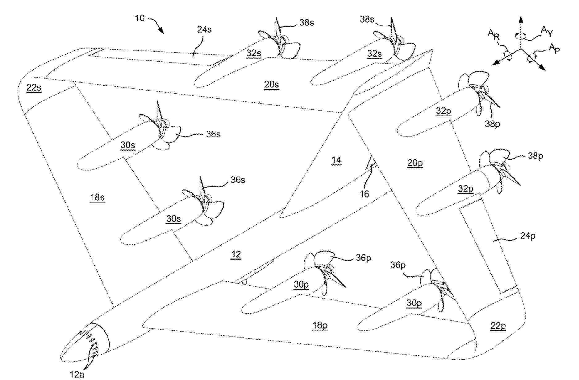
Submersible box-winged vehicle systems generate hydroelectric energy using naturally occurring tidal flows and/or water currents in a body of water. The vehicle systems include a submersible hull, an upright dorsal fin extending from an aft portion of the submersible hull, port and starboard wing assemblies each having respective proximal ends joined to a forward region of the hull an and an upper region of the dorsal fin so as to establish a box wing configuration, and electrical power generation units attached to the port and starboard wings, wherein each of the electrical power generation units include a generator and a marine propeller operatively connected to the generator so as to cause the generator to generate electrical energy in response to the marine propeller turning. The vehicle system when submerged in a body of water thereby allows tidal flows and/or currents associated with the body of water to responsively turn the marine propeller of each of the electrical power units thereby generating electricity by the generator operably associated therewith
Resumen de: EP4799916A2
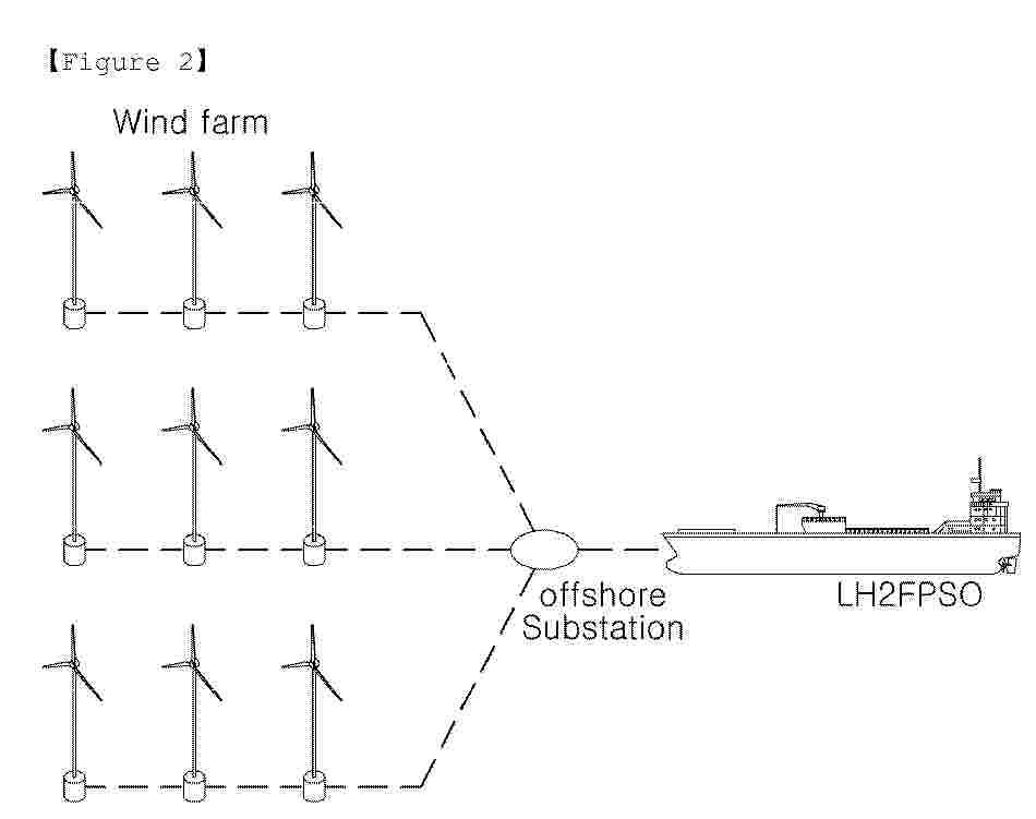
The present invention relates to an apparatus and method for producing, storing, and transferring hydrogen. According to the present invention, in order to address the problems of conventional systems and methods for producing, storing, and transferring marine green hydrogen, which are configured with a fixed structure in a small-scale offshore wind power generator on a coast or in a shallow sea area with a shallow depth of water, and thus, have low efficiency due to the difficulty in mass production of hydrogen, and a large storage space is occupied when the produced hydrogen is converted into a compressed gas form, and when the produced hydrogen is converted into ammonia, additional energy is required to extract the hydrogen again and there is a risk of environmental pollution and casualty in the event of an outflow accident, provided is a marine platform for producing, storing, and transferring marine green hydrogen, which is configured such that marine green hydrogen is produced through a floating marine structure configured to produce marine green hydrogen using electricity produced using renewable energy from the ocean, and simultaneously, the produced marine green hydrogen is stored, transferred, and offloaded through a single offshore platform (FPSO), thereby being possible to easily construct a large-scale production facility capable of producing, storing, and transferring marine green hydrogen without greenhouse gas emission on the basis of eco-friendly energy.
Nº publicación: AU2026214078A1 27/08/2026
Solicitante:
TECHNIP ENERGIES FRANCE
TECHNIP ENERGIES FRANCE
Resumen de: AU2026214078A1
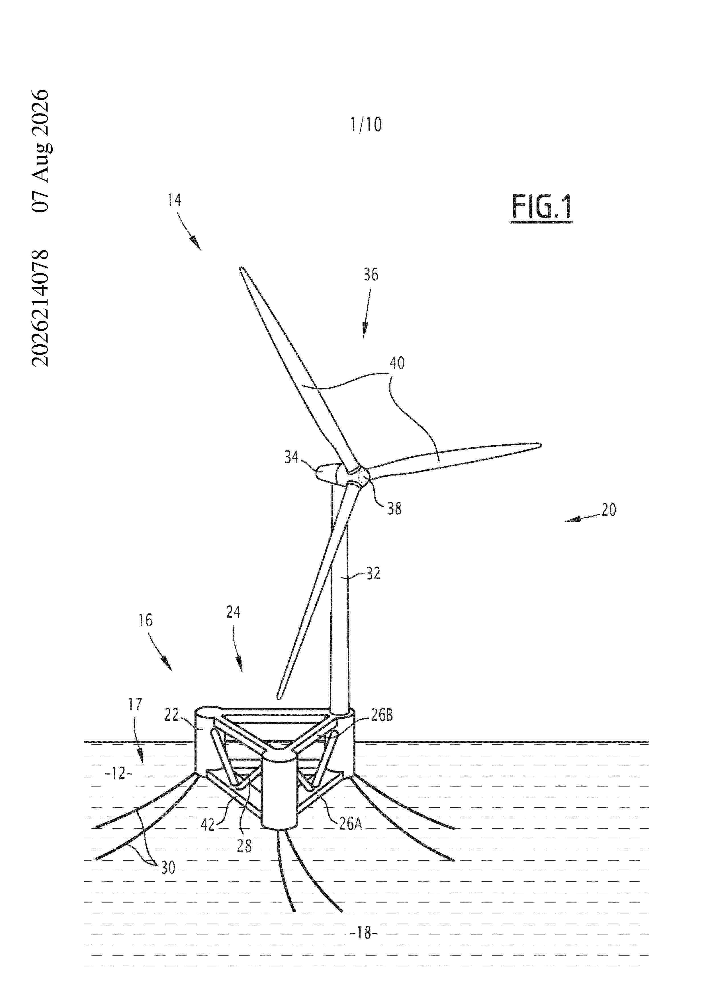
Offshore floating intervention platform having a lifting tower with a position compensation device, related assembly and method The intervention platform (10) comprises at least a wind turbine equipment lifting tower (100), having at least a lifting unit (110A, 110B) comprising : a mast (112), a wind turbine equipment elevator (114) configured to vertically move along the mast (112) between a lower loading/unloading position and at least an upper intervention position and a lifting actuator (116), configured to move the wind turbine equipment elevator (114) between the lower unloading/loading position and the upper intervention position. The lifting unit (110A, 110B) comprises at least a position compensation device (118) configured to be activated in the loading/unloading position and/or in the intervention position to compensate local vertical displacements between the intervention platform (10) and the wind turbine platform when the intervention platform (10) is docked to the wind turbine platform. Figure 6 and ug u g a n d F' rx 140, 142 40 ug u g
 BOPI
BOPI
 Sede Electrónica