Si deseas distinguir tus productos, servicios o ambos de los de otra empresa, es posible que necesites una marca o nombre comercial. Descubre qué son, en qué consiste su procedimiento de registro y qué implica.

Información sobre los plazos de presentación de solicitudes de transformación de marcas de la Unión Europea en marca nacional española. Más información


Si tienes un nuevo dispositivo, producto o procedimiento que resuelva un problema técnico o tenga una ventaja práctica, existen distintas formas de protegerlo en España y en otros países. Descubre cómo hacerlo.

¿Tu innovación reside en la estética, la ornamentación o la apariencia de tu producto? Protégela mediante un diseño industrial. Descubre qué derechos confiere el registro y cómo realizar la tramitación.

Las indicaciones geográficas protegen el nombre de un producto originario de una zona geográfica, a la cual le debe una determinada calidad, reputación u otra característica. Descubre qué son, en qué consiste su procedimiento de registro y qué beneficios conceden.

Las patentes publicadas en todo el mundo son una valiosa fuente de información científica, técnica y comercial.

Si eres emprendedor/a o una empresa y quieres potenciar y mejorar la rentabilidad de tu negocio protegiendo de forma adecuada los activos intangibles de tu organización, en este espacio encontrarás lo necesario.


 85
resultados
85
resultados
 Última actualización
24/04/2026 [06:58:00]
Última actualización
24/04/2026 [06:58:00]


Resumen de: WO2026077538A1
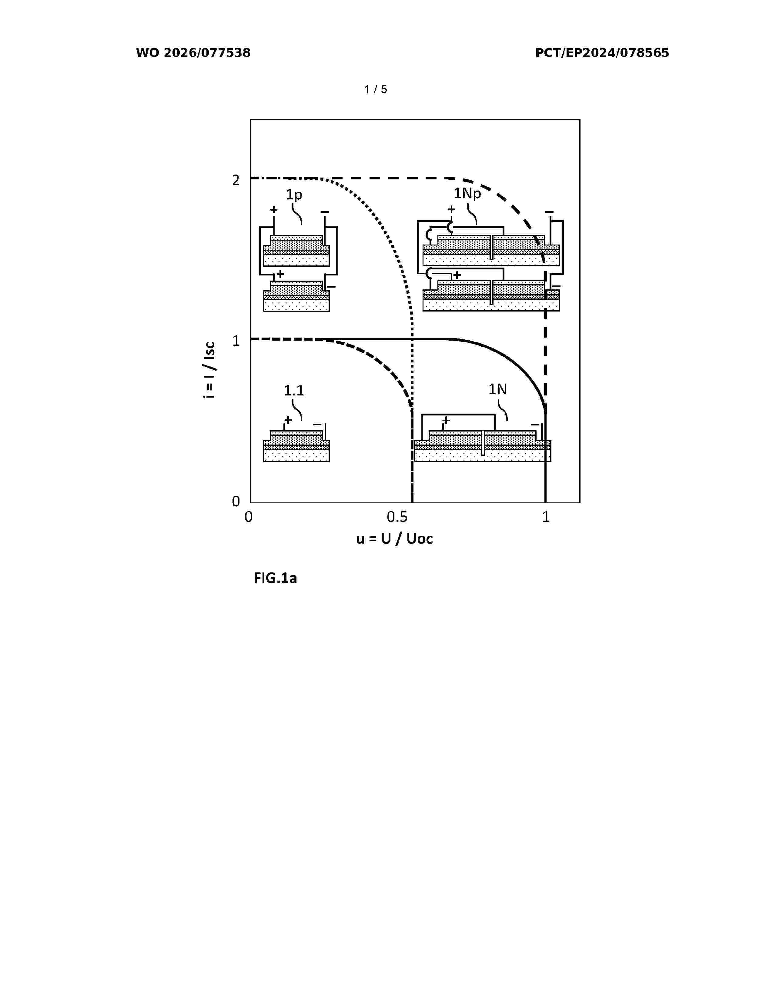
A photovoltaic power converter (1N) suitable for use in implanted AIMD's is provided which comprises an insulating substrate (5s) supporting N photovoltaic cells (= PV-cell) (1.1-1.N) physically separated from one another by gaps and conductively coupled in series to one another, wherein N ≥ 2. A blocking layer (4b) is interposed between each of the N PV-cells and the insulating substrate (5s) to reduce photo-leakage caused by photoconductivity of the insulating substrate (5s). Each blocking layer (4b) is formed by M blocking PN-junctions, wherein M ≥ N + 1, each formed between a pair of first and second type p and type n semiconductors (4pi, 4ni, with i = 1 to M), wherein the first blocking PN-junction located closest to the photovoltaic PN-junction has a second polarity of opposite sign from the polarity of the PN junction of the PV cell.

Resumen de: WO2026077387A1
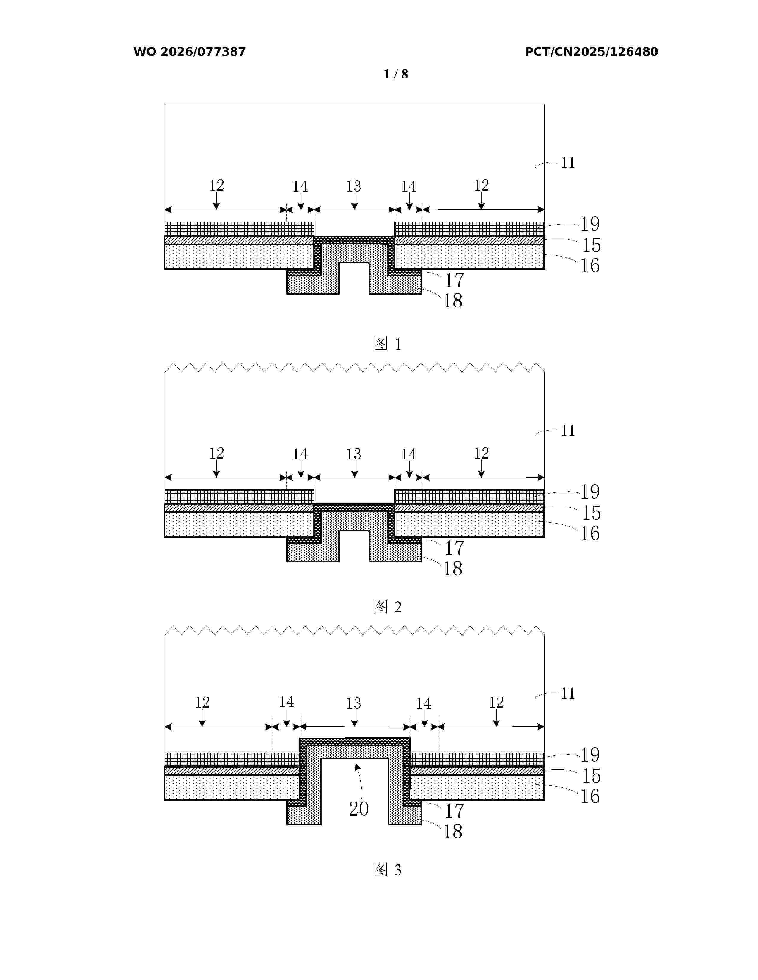
The present application relates to the technical field of photovoltaics, and discloses a back contact cell and a photovoltaic module. Field passivation is performed on a first region and an overlapping region by means of a doping layer, and the doping layer can form a favorable electric field consistent with the induction direction of a first doped silicon layer, thereby improving charge carrier collection efficiency of the first doped silicon layer. The back contact cell comprises a semiconductor substrate, a tunneling passivation layer, a first doped silicon layer, an intrinsic silicon layer, a second doped silicon layer, and a doping layer. The tunneling passivation layer and the first doped silicon layer are sequentially stacked on the first region and the overlapping region. The intrinsic silicon layer and the second doped silicon layer are sequentially stacked on a second region, and further extend onto a first interface passivation layer and the first doped silicon layer located in the overlapping region. The doping layer is disposed within the first region and the overlapping region of the semiconductor substrate. The doping concentration of a first doping element in the doping layer having the same conductivity type as the first doped silicon layer is greater than the doping concentration of a first doping element in the second region of the semiconductor substrate.
Resumen de: WO2026079660A1
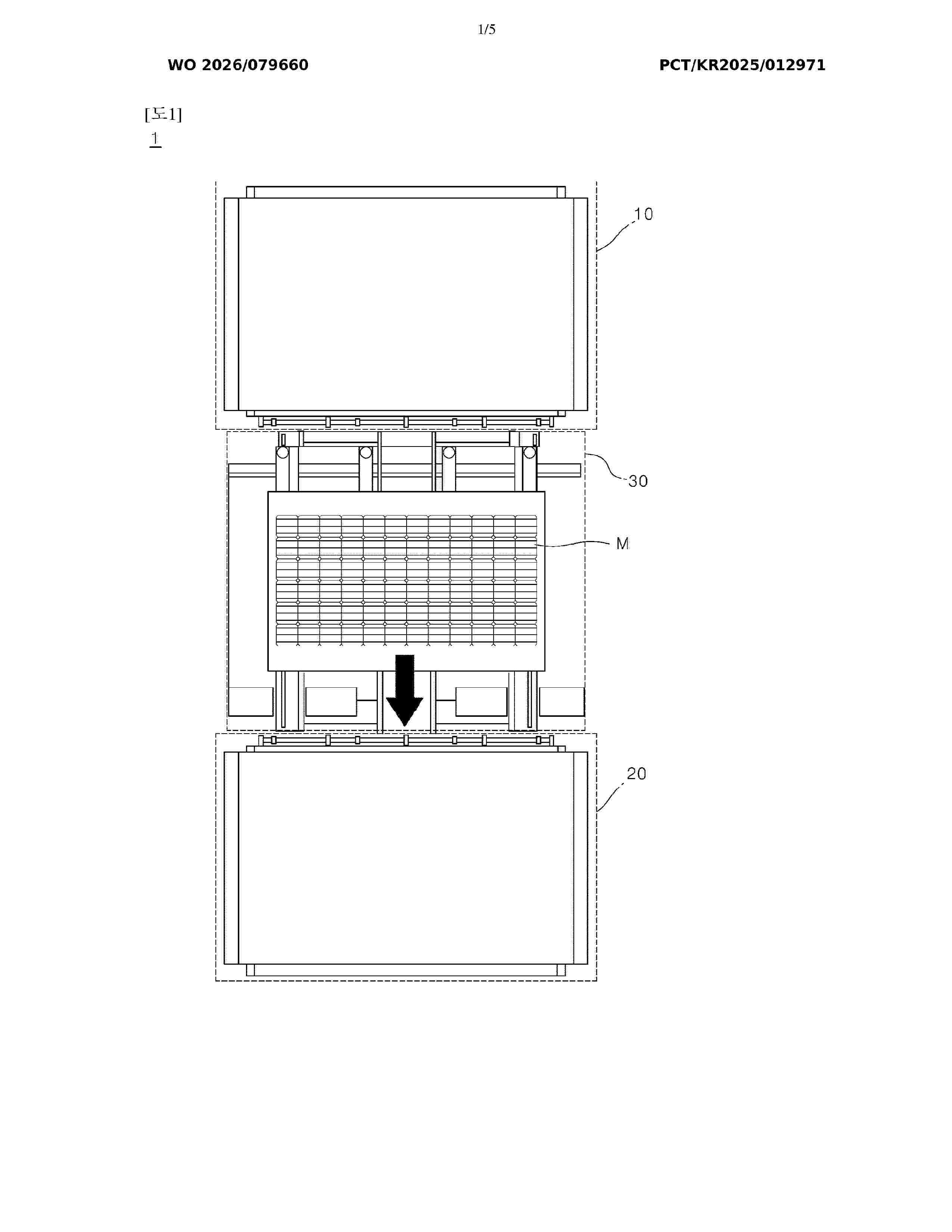
The present invention provides a solar cell module laminator, comprising: a laminating chamber including a space for accommodating a solar cell module, and a heating unit and a vacuum unit; and a conditioning chamber including a seating unit on which the laminated solar cell module is seated, and a press unit aligned with the seating unit and in close contact with one surface of the solar cell module.
Resumen de: DE102024129971A1
Die Erfindung betrifft ein Photovoltaikmodul mit einer Vorderseite, einer Rückseite, einem Photovoltaikelement, einer Schutzstruktur und einem elektrischen Anschluss, wobei die Schutzstruktur das Photovoltaikelement zum Schutz flächig überdeckt und wobei das Photovoltaikelement einstrahlendes Licht in elektrische Leistung umsetzt und die elektrische Leistung am elektrischen Anschluss bereitstellt, wobei das Photovoltaikmodul mittels zumindest einem an der Rückseite fixierten Stützprofil entlang einer Stützprofillängsachse und einem entlang der Stützprofillängsachse verlaufenden Stützprofilquerschnitt durch eine Steifigkeit des Stützprofils gegen Verformung gestützt ist, wobei der Stützprofilquerschnitt ausgehend von einem Mittelbereich einen ersten Profilschenkel mit einem ersten Endbereich und einen zweiten Profilschenkel mit einem zweiten Endbereich ausbildet, wobei der erste Endbereich und der zweite Endbereich an der Rückseite des Photovoltaikmoduls fixiert sind und am Mittelbereich eine durch eine Länge der Profilschenkel von der Rückseite beabstandet angeordnete Montagefläche zum Montieren des Photovoltaikmoduls an einem Untergrund ausgebildet ist. Des Weiteren betrifft die Erfindung eine Photovoltaikanlage sowie ein Verfahren zum Montieren eines Photovoltaikmoduls.
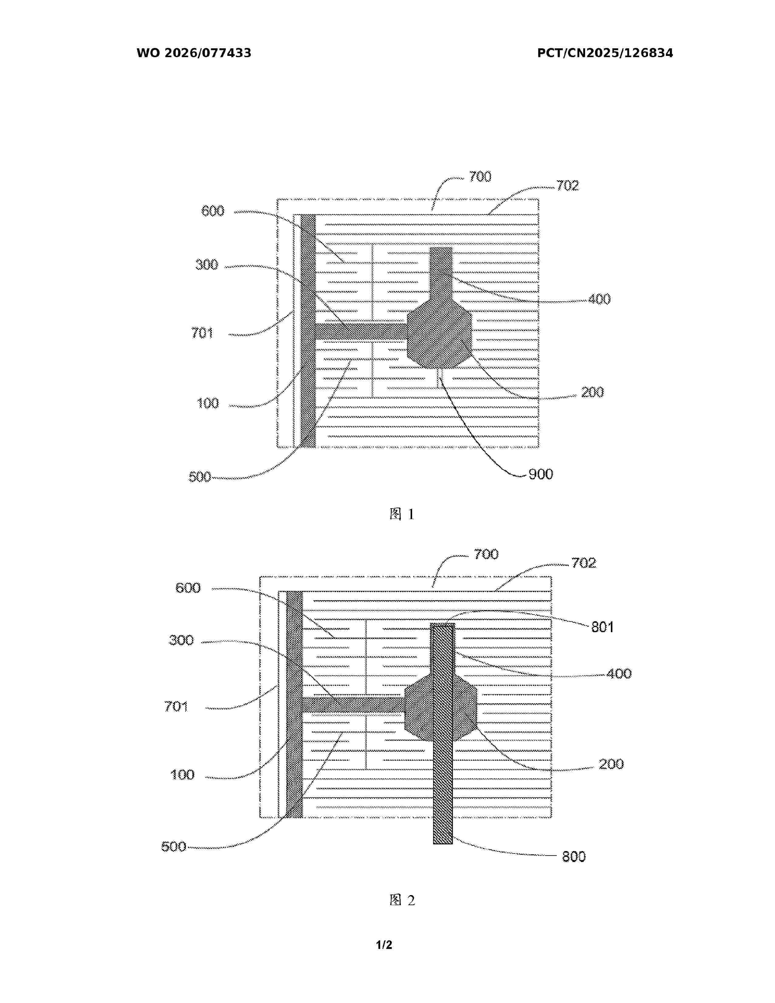
Resumen de: WO2026077433A1
The present disclosure is applicable to the technical field of photovoltaics. Provided are an electrode structure, a cell and a module. The electrode structure comprises: a main grid closest to a first edge of a back-contact cell; pad points spaced apart from the main grid in a first direction; a first connection grid line which comes into electrical contact with the pad points and the main grid; and a second connection grid line having a first end which comes into electrical contact with the pad points and a second end extending in a second direction.
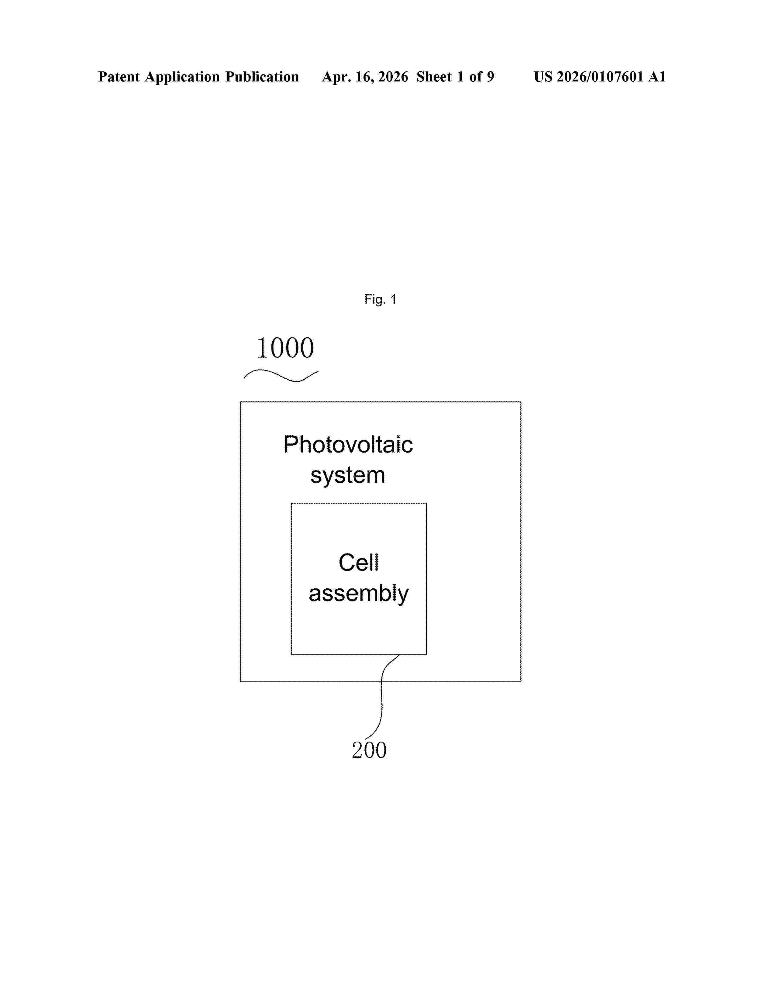
Resumen de: US20260107601A1
In a back electrode structure of a back-contact solar cell, first fingers include first finger pre-plating layers forming ohmic contact with a substrate and first finger electroplating layers plating the first finger pre-plating layers, and second fingers include second finger pre-plating layers forming ohmic contact with the substrate and second finger electroplating layers plating the second finger pre-plating layers. First busbars are in contact with the first finger pre-plating layers, the first fingers are disconnected at second busbars, and the second busbars are in contact with the second finger pre-plating layers. First/second conductive connectors are arranged at two ends of the first/second busbars, respectively. The first conductive connector is connected to ends of all the first busbars facing away from the second conductive connector, and the second conductive connector is connected to ends of all the second busbars facing away from the first conductive connector.
Resumen de: AU2025238104A1
Embodiments of the present application relates to the technical field of photovoltaics, and in particular, to a solar cell and a photovoltaic module to solve the problem that a side surface of a solar cell in the related art cannot balance a light trapping effect and passivation performance. The solar cell includes a silicon substrate and a passivation layer. The silicon substrate includes a first surface and an opposite second surface, and a plurality of side surfaces connecting the first surface and the second surface. At least one of the side surfaces includes a plurality of first texture regions and second texture regions. The first texture region includes a plurality of first pyramid structures. The second texture region includes a plurality of second pyramid structures. A structural dimension of the second pyramid structure is greater than a structural dimension of the first pyramid structure. The second texture regions are formed between adjacent first texture regions. The passivation layer covers the first texture regions and the second texture regions of at least one of the side surfaces. Embodiments of the present application relates to the technical field of photovoltaics, and in particular, to a solar cell and a photovoltaic module to solve the problem that a side surface of a solar cell in the related art cannot balance a light trapping effect and passivation performance. The solar cell includes a silicon substrate and a passivation layer. The silicon substrate i
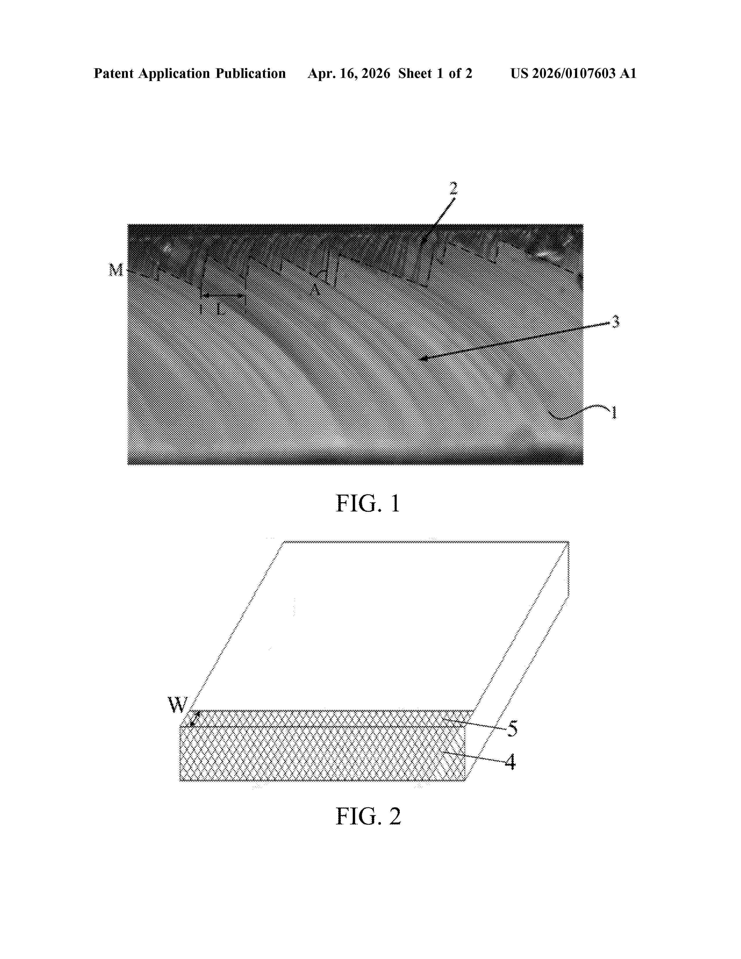
Resumen de: US20260107603A1
This application discloses a solar cell and a photovoltaic module. In one example, a solar cell includes a first surface and a second surface opposite to each other, and a side surface connecting the first surface and the second surface. The side surface includes a cut surface, the cut surface including a cut edge adjacent to the first surface and a break edge adjacent to the second surface. A first passivation layer is formed on the cut surface. The first passivation layer includes an aluminum oxide passivation layer. The cut surface includes a first region adjacent to the cut edge and a second region farther away from the cut edge than the first region. A ratio of oxygen to aluminum in at least a part of the first region is greater than a ratio of oxygen to aluminum in at least a part of the second region.
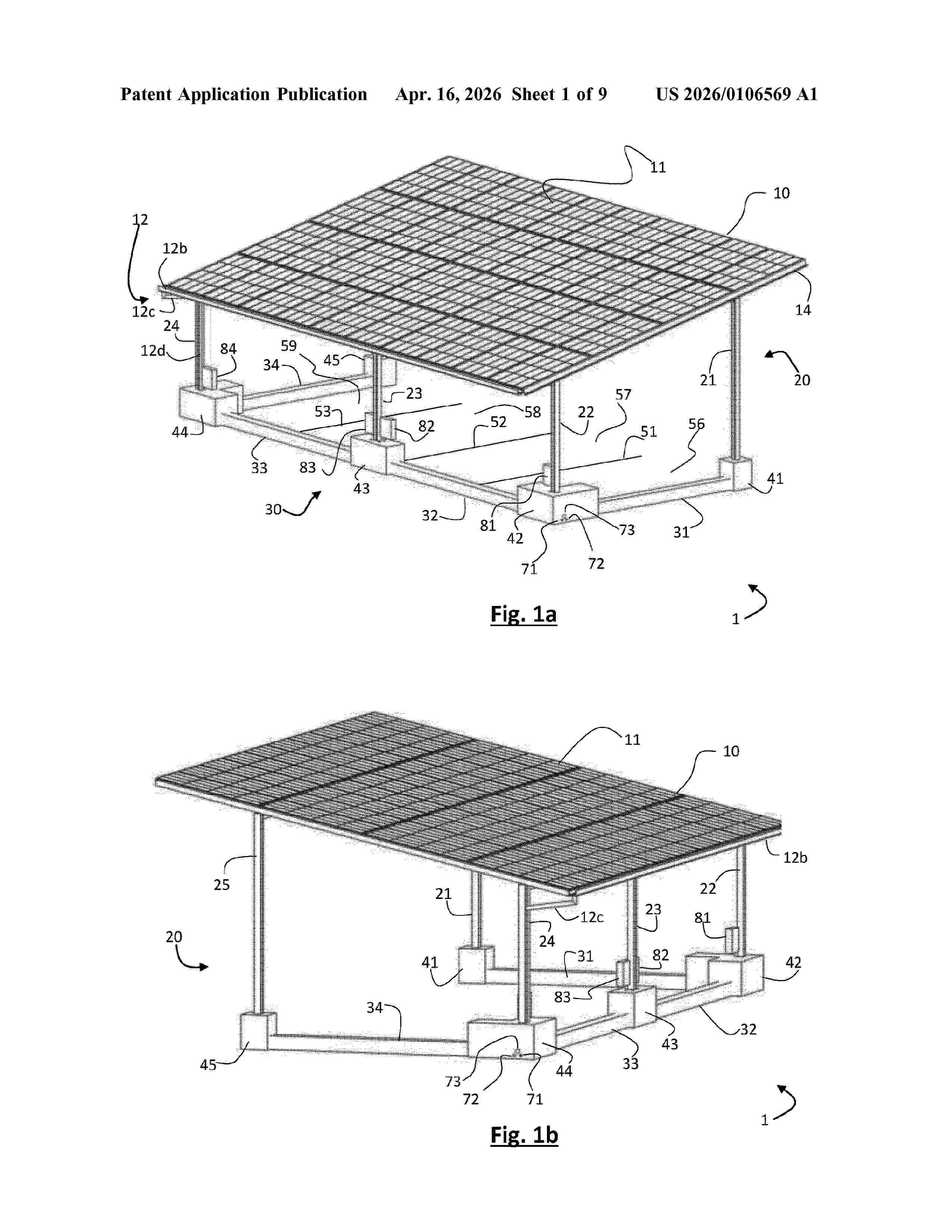
Resumen de: US20260106569A1
A system for supporting a roof, e.g. for a carport or canopy, said roof comprising one or more PV panels, the system comprising a vertical support frame, wherein the vertical support frame comprises one or more vertical supports, is configured to support the roof; a base frame, wherein the base frame is configured to support the vertical support frame, is configured to be arranged on a foundation-free ground surface, comprises a plurality of horizontal supports, wherein at least one of the horizontal supports is a multifunctional support which comprises concrete; is a structural component; and comprises an internal electricity channel for an electrical base cable configured to be electrically connected to the PV panel.
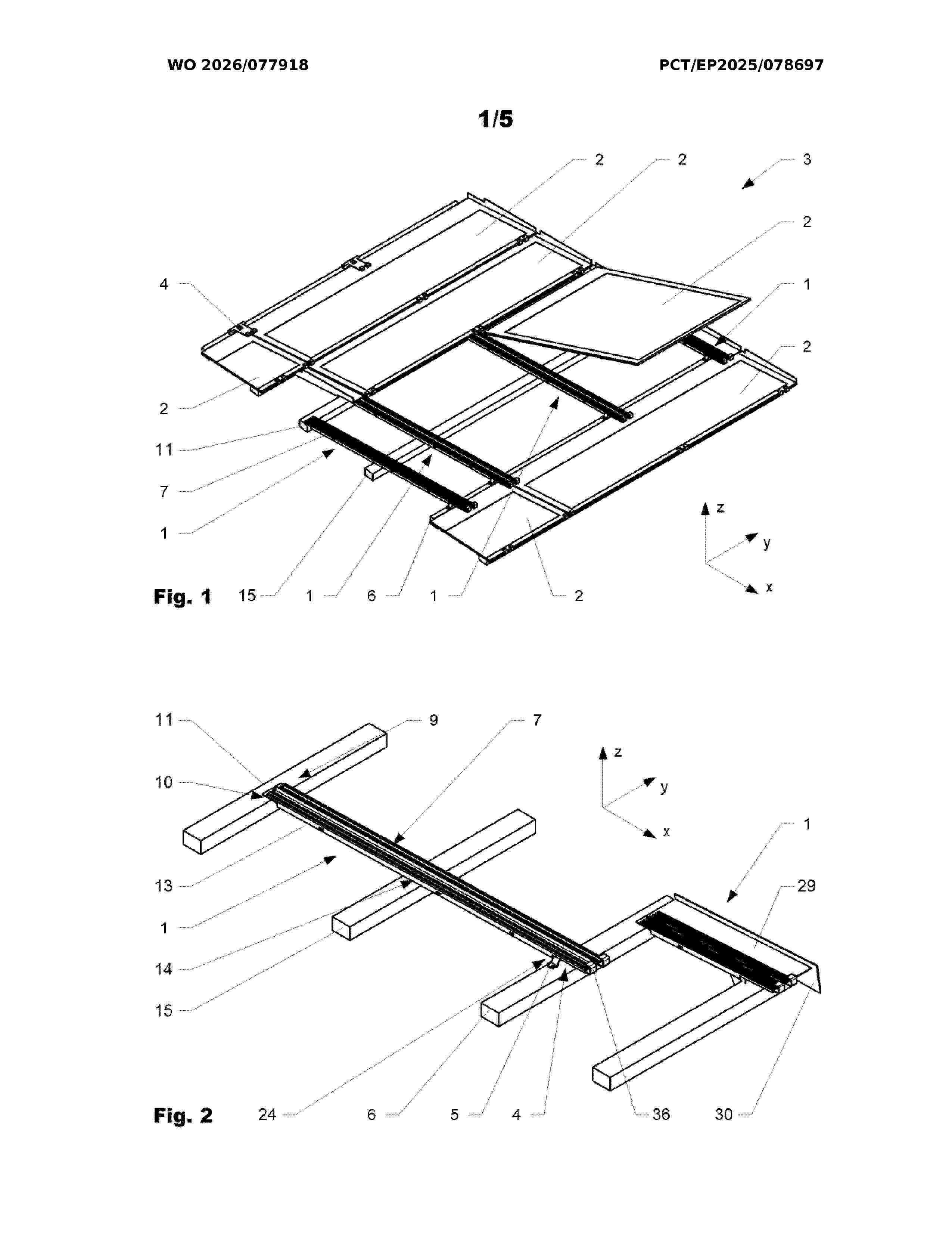
Resumen de: WO2026077918A1
The disclosure relates to a holder (1) for a solar roof tile (2) on a tilted roof (3) comprising a base (4) comprising a lower support (5) supported in the mounted position on a lower batten (6) of the tilted roof (3) and an oblong beam (7) extending in a longitudinal direction x. The oblong beam comprises a lower end (8) interconnected in the mounted position to the base (4); an upper end (9) comprising an upper support (10) which in a mounted position is supported by an upper batten (11) of the tilted roof (3); a bearing surface (12) for supporting in the mounted position at least one solar roof tile (2) with respect to the upper batten (11) and the lower batten (6); and at least one stiffening fin (13) protruding from the oblong beam (7) in a normal direction z generally perpendicular to the longitudinal direction x for increasing the resistance of the oblong beam (7) against bending.
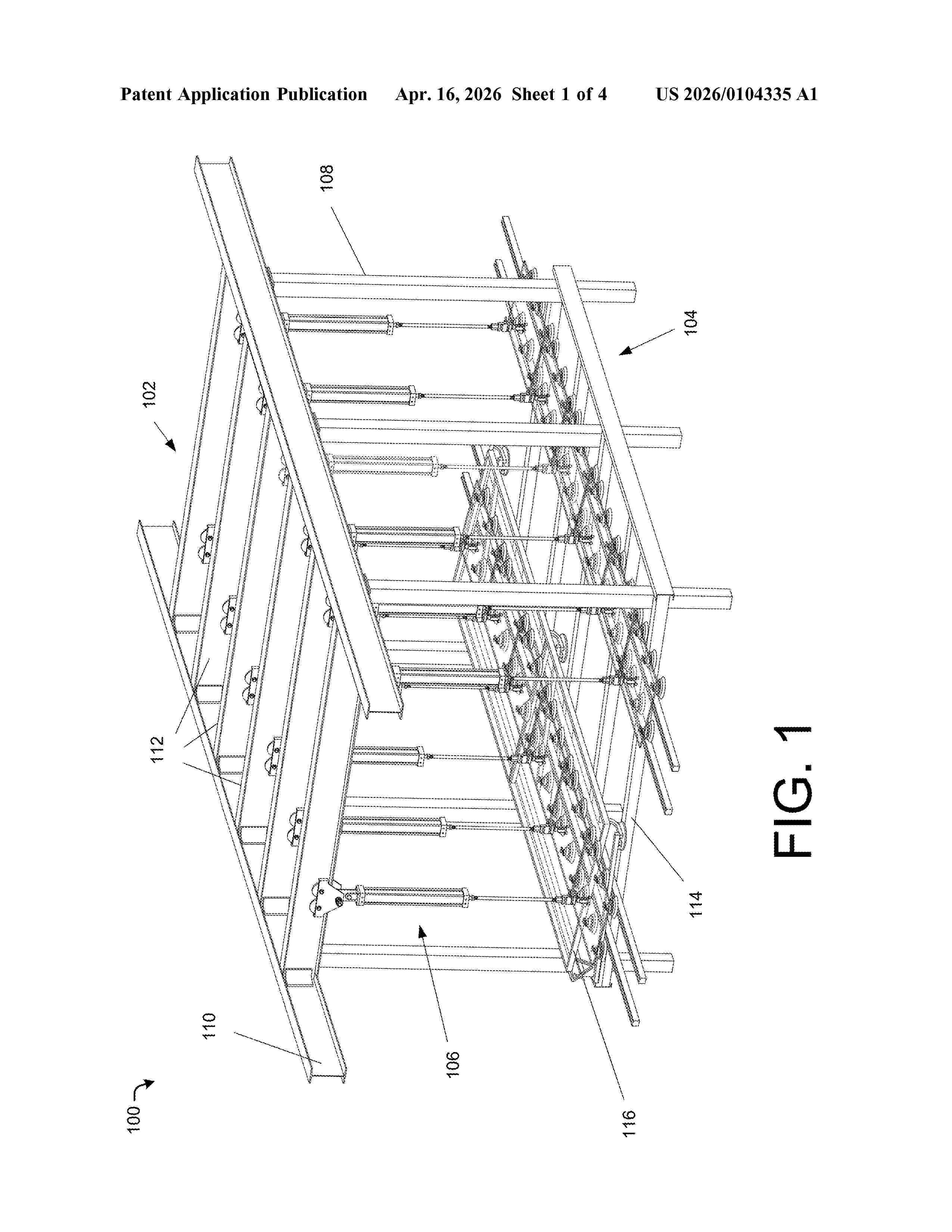
Resumen de: US20260104335A1
An apparatus for testing solar panel modules that includes a support frame, a test bed fixedly connected to the support frame and configured to connect with a solar panel module, and a load testing device mounted to the support frame. The load testing device includes a positioning device mounted to the support frame, an actuator hingedly fastened to the positioning device, and an arm having a first end rigidly fastened to the actuator and a second end opposite the first end. The arm extends away from the actuator. A load cell is fastened to the second end of the arm, and a universal joint is fastened to the load cell. A plate is hingedly connected to the universal joint, and a suction cup is rigidly engaged with the plate. A pneumatic system connection is incorporated within the actuator, and a vacuum system connection is incorporated within the suction cup.
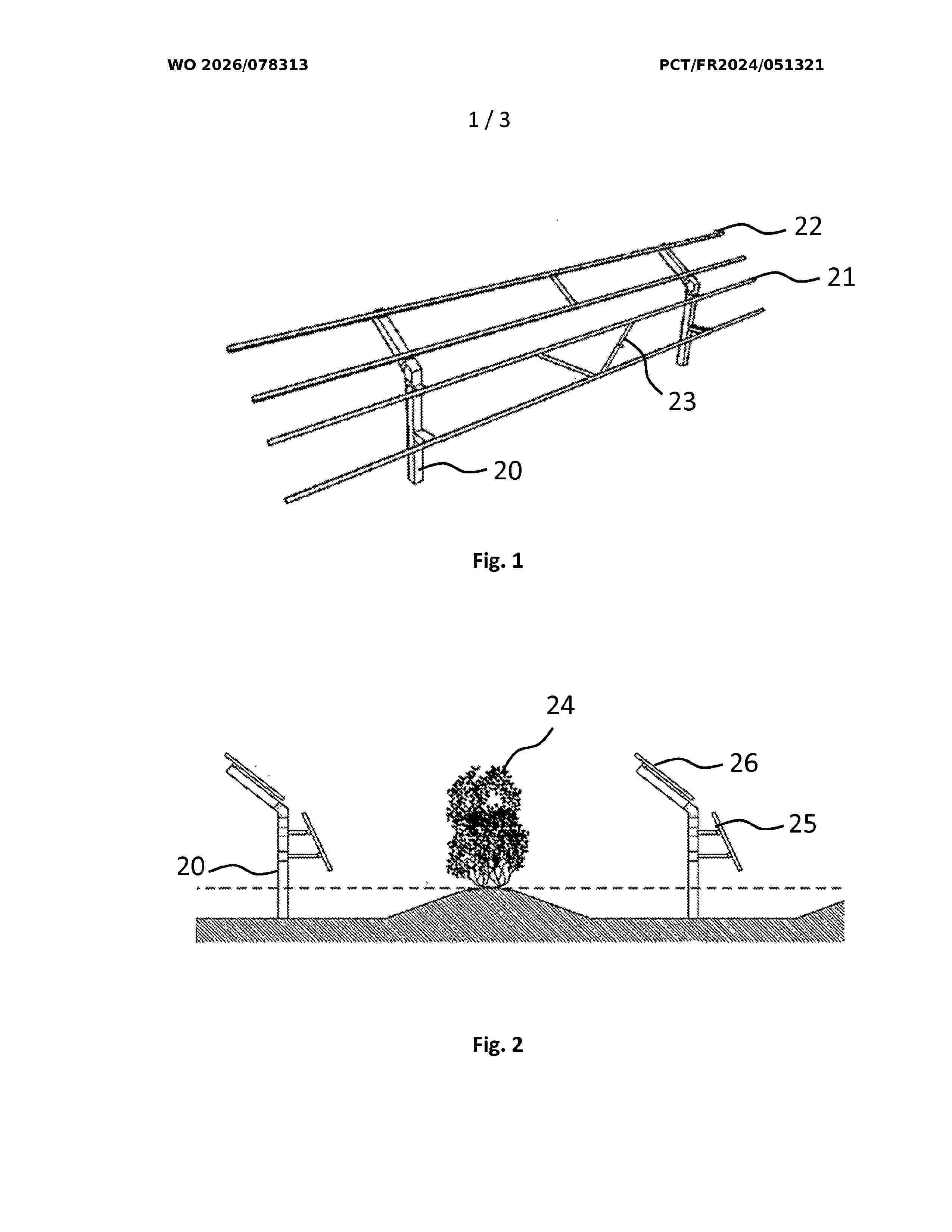
Resumen de: WO2026078313A1
The invention relates to a protective and energy-producing element for a plantation, characterized in that it comprises: at least two support posts (20) intended to be secured to the plantation soil, each having at least one portion proximal to the ground with a given orientation with respect to the vertical, the posts having a portion distal to the ground; at least two first longitudinal crossmembers (21) arranged on either side of the at least two posts (20); at least one first photovoltaic panel arranged along the first support plane; at least two second longitudinal crossmembers (22) arranged on either side of the at least two posts (20); and at least one second photovoltaic panel arranged along the second support plane.
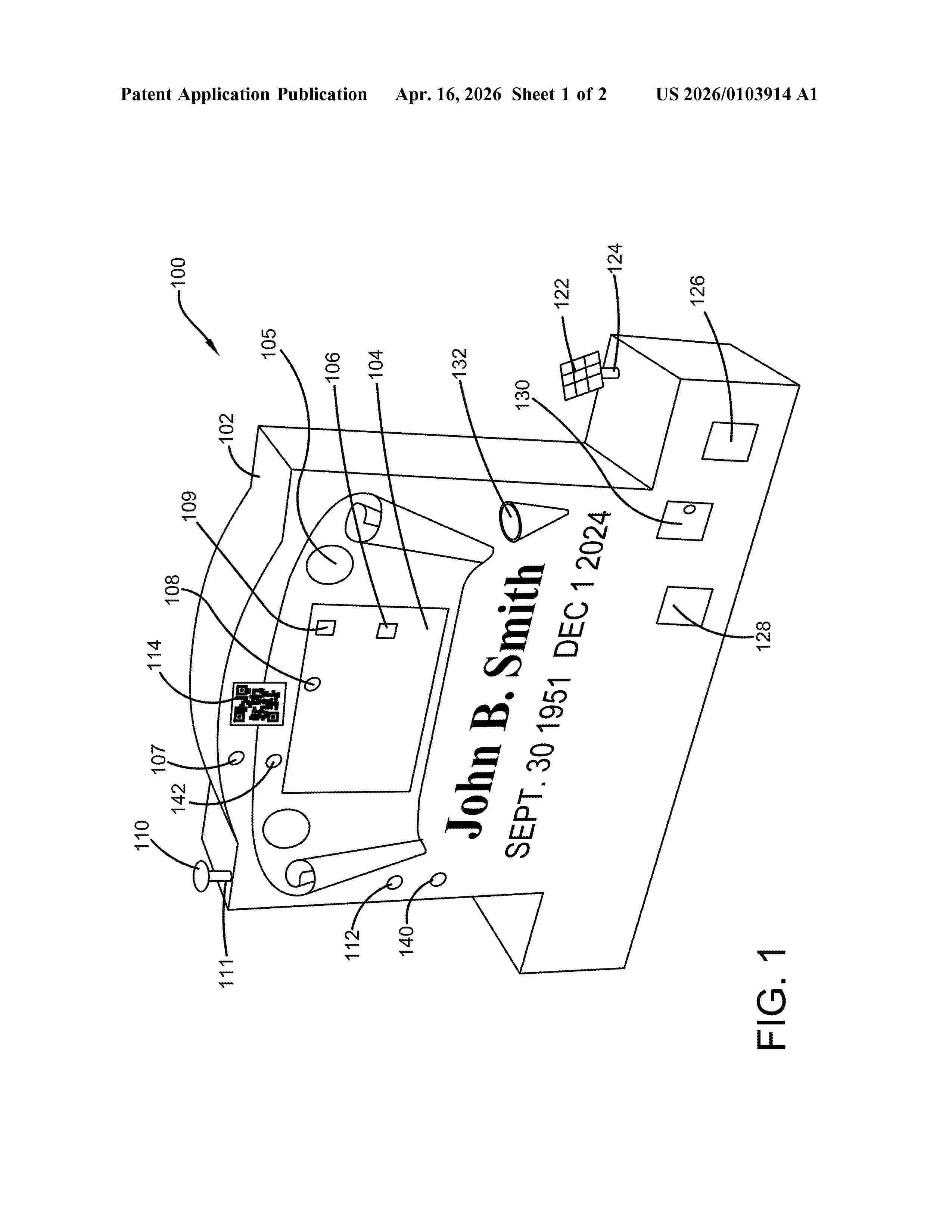
Resumen de: US20260103914A1
An electronic tombstone device is provided. The device is comprised of a multifunctional tombstone device designed to enhance personalization, interactivity, and durability for outdoor applications. The device comprises a body featuring an LED display with anti-glare, scratch-resistant, and oleophobic treatments to support media playback in diverse orientations. Integrated lighting provides aesthetic and functional illumination, including customizable modes such as motion-activated or candlelight effects. The device also incorporates weatherproof speakers for personalized audio playback and motion sensors for triggering interactive features like media displays and lighting. Media uploads are facilitated via a secure, weather-resistant QR code leading to a password-protected webpage. Power options include solar panels with energy storage or alternative wired solutions. Additional features include motion-activated animal deterrents, protected storage compartments for tributes, and integrated vases with drainage systems, ensuring functionality and respect for memorial environments.
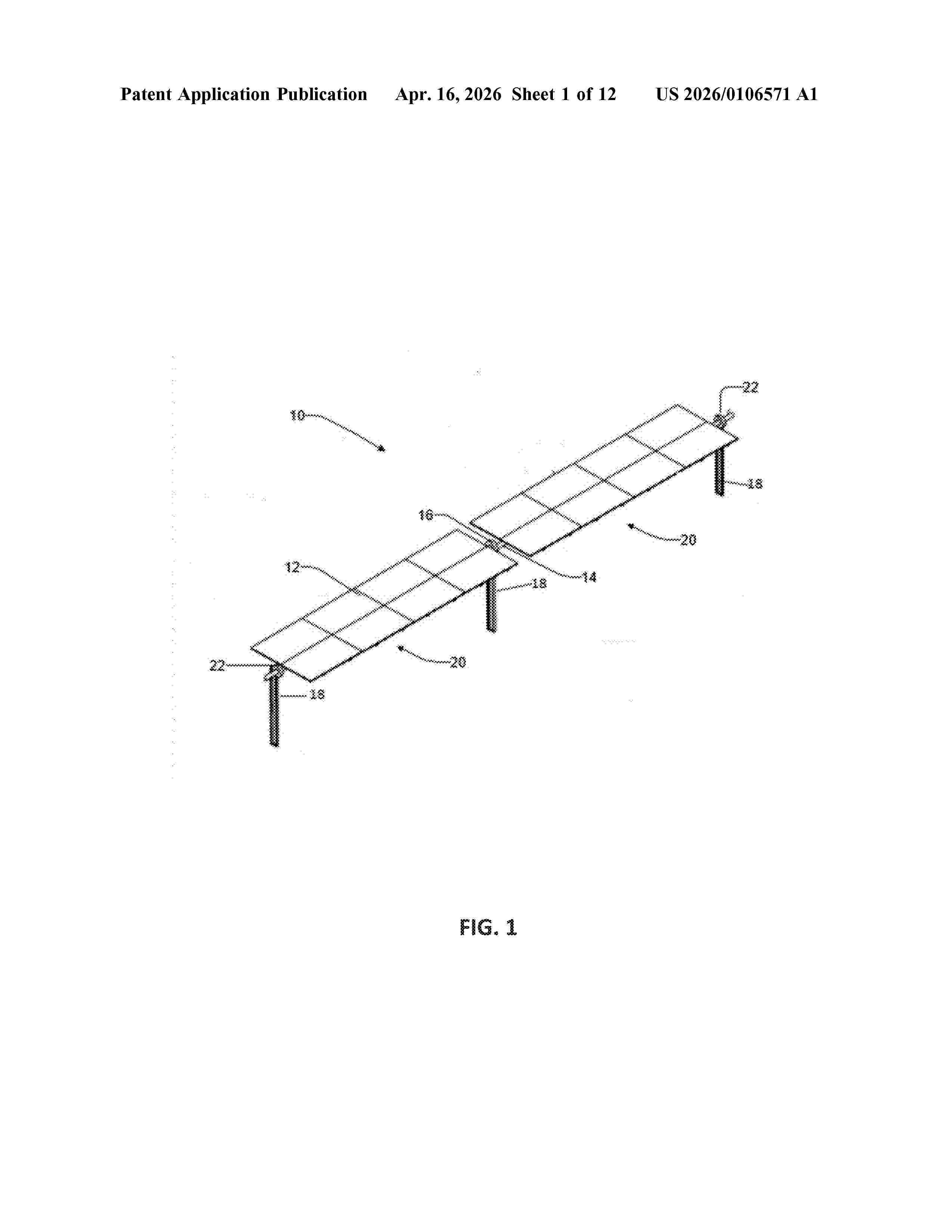
Resumen de: US20260106571A1
A solar tracking system including a plurality of solar tracker rows arranged in parallel in a north-south direction wherein each solar tracker row may include a plurality of support piers, a torque tube extending along the row in the north-south direction rotatably supported on the plurality of support piers, a plurality of solar modules coupled to the torque tube, and a plurality of dampers. A first set of support piers of the plurality of support piers each include one or more dampers of the plurality of dampers, and the first set of piers forming a repeating pattern of support piers along the plurality of support piers in the solar tracker row.
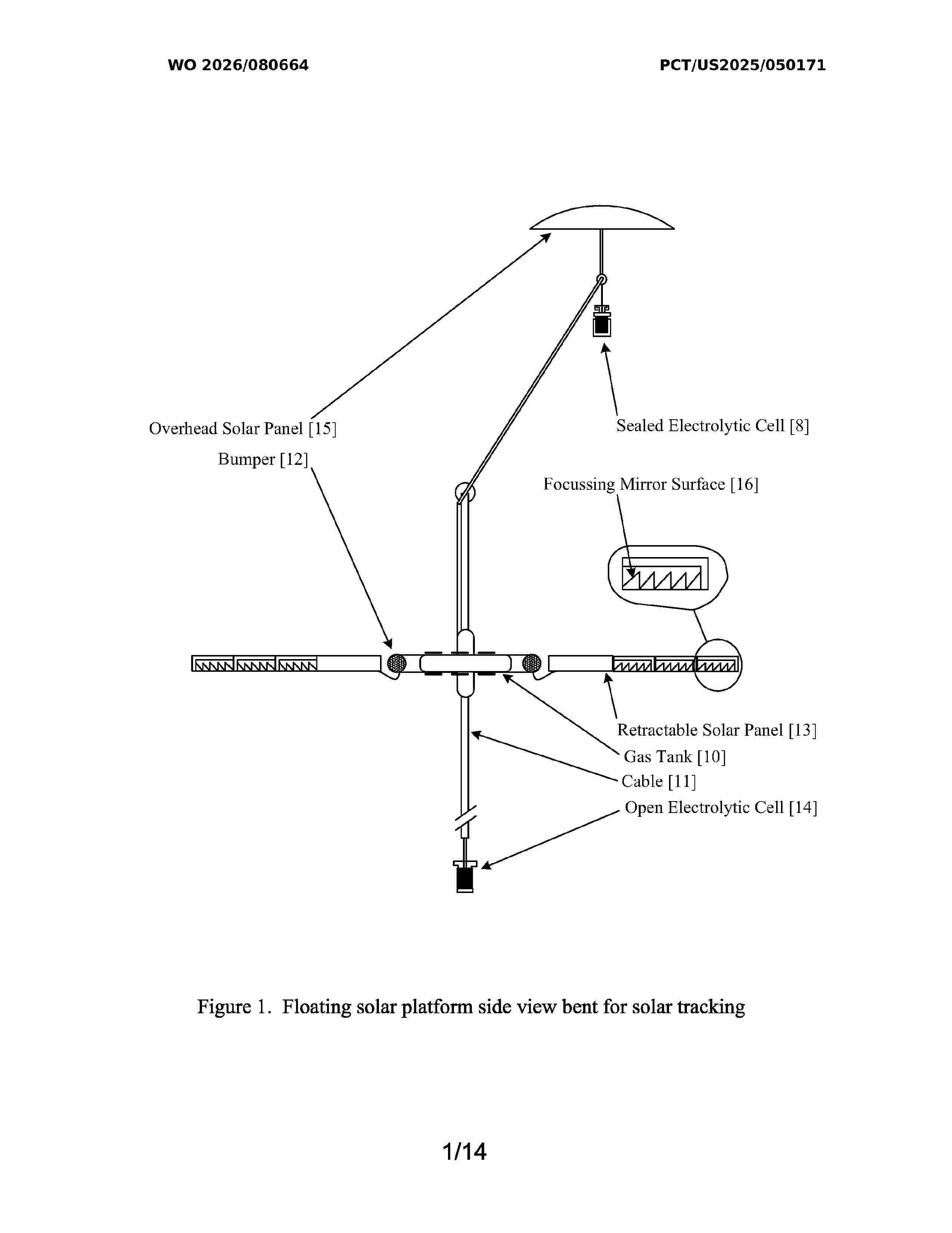
Resumen de: WO2026080664A1
Large scale harvesting of renewable energy is proposed by using floating devices which use solar, wind, ocean current, and wave energy to produce compressed hydrogen by electrolysis of deep sea water. Natural ocean currents and winds are used to allow the devices to gather energy from over a large area with minimum transportation cost. The present approach uses a combination of well understood technologies in an optimized manner and at scale. Hydrogen produced in this manner would pave the way for carbon free energy economy.
Resumen de: DE102024129905A1
Die Erfindung betrifft ein Vorrichtung (10) zum Umwandeln von Solarenergie in elektrische Energie und Wärmeenergie, die Vorrichtung (10) umfassend: einen Grundkörper (12) mit einer zur Sonne ausrichtbaren Oberseite (14), einer zu einem Gebäude (16) ausrichtbaren Unterseite (18) und wenigstens eine zwischen der Oberseite (14) und der Unterseite (18) angeordnete Mantelseite (20); ein die Oberseite (14) bildendes Photovoltaikmodul (24) zum Umwandeln der Solarenergie in elektrische Energie; und ein Wärmetauscher (28) mit einem Fluidraum (44), welcher von einem Wärmefluid (46) durchströmbar ist, wobei der Fluidraum (44) an das Photovoltaikmodul (24) angrenzt.
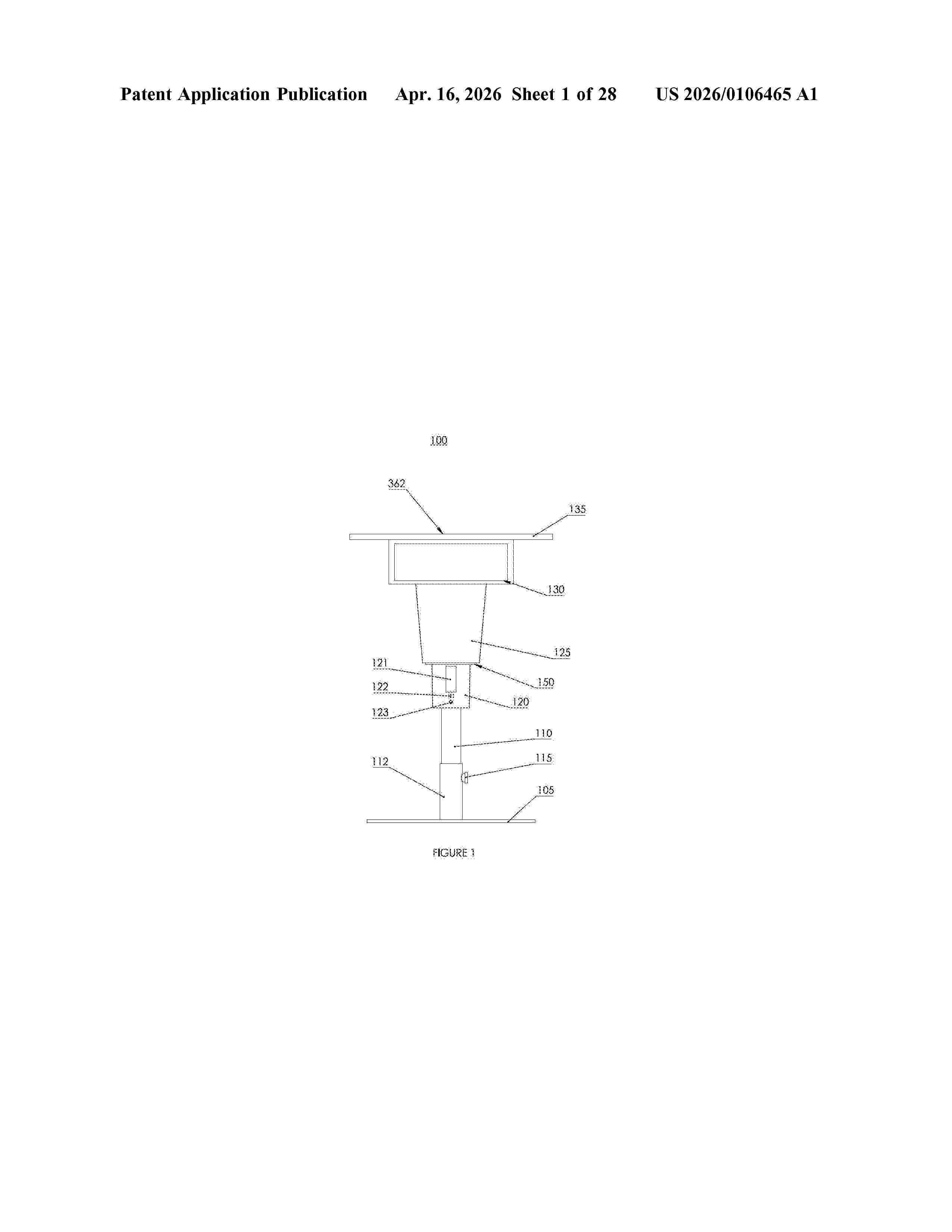
Resumen de: US20260106465A1
A solar-powered table including a base unit and a top section detachably coupled or connected to the base unit. The top section includes one or more solar cell assemblies including one or more solar cells, the one or more solar cells to receive light from a solar light source and convert the light to electrical energy; one or more battery charge controllers coupled to the one or more solar cell assemblies and one or more rechargeable batteries to receive the electrical energy and to transfer the electrical energy to charge the one or more rechargeable batteries; and one or more processors or controllers.
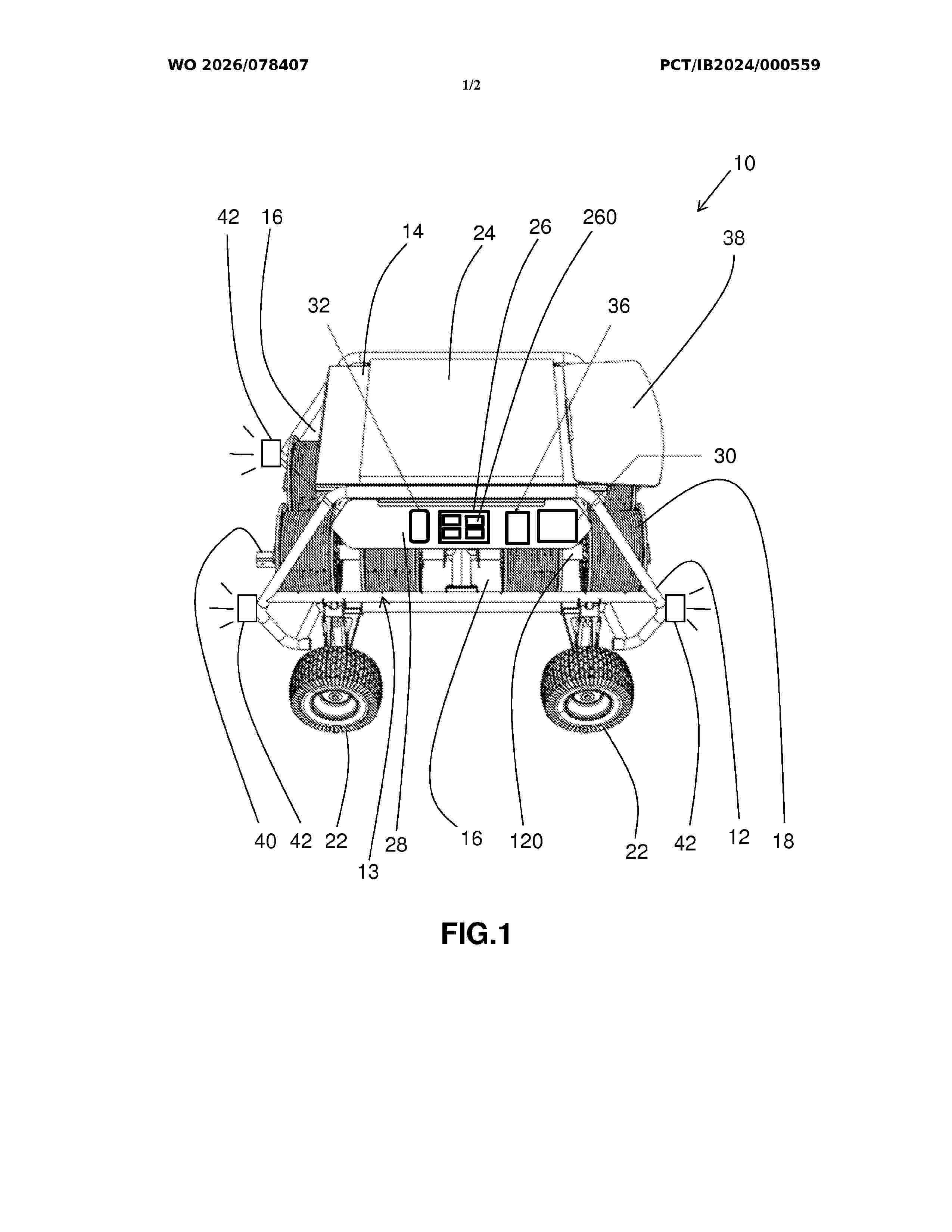
Resumen de: WO2026078407A1
This mobile unit (10) for transporting and installing electric cables comprises: a chassis (12) delimiting a roof (14) on top of the mobile unit (10) and an opening (16) on each side of the mobile unit (10), the chassis (12) comprising at least one shaft (120) parallel to the driving direction of the mobile unit (10) and adapted to receive at least one cable drum (18) free to rotate about the shaft (120) for unwinding cable through the openings (16); an electric motor for driving the mobile unit (10); at least four wheels (22) or two tracks, two of the four wheels (22) or one of the two tracks being arranged on opposite sides of the mobile unit (10); and at least one photovoltaic panel (24) mounted on the roof (14) and supplying the electric motor with solar energy for driving.
Resumen de: DE102024129671A1
Die Erfindung betrifft eine Solarmodulmontagehilfe zum temporären Fixieren eines Öffnungswinkels eines an einer im Wesentlichen horizontal angeordneten Solarmodulhalterung angeordneten Solarmoduls, eine Solarmodulanordnung, eine Solaranlage, ein Verfahren sowie eine Verwendung der Solarmodulmontagehilfe. Die Solarmodulmontagehilfe ist insbesondere stabförmig ausgestaltet und weist an einem ersten Ende eine erste Befestigungseinrichtung zum temporären Anordnen der Solarmodulmontagehilfe an der Solarmodulhalterung und an einem dem ersten Ende gegenüberliegend angeordneten zweiten Ende eine zweite Befestigungseinrichtung auf. Eine Länge der Solarmodulmontagehilfe ist mittels eines Verstellmittels verstellbar und temporär arretierbar. Die Solarmodulmontagehilfe ist eingerichtet, das Solarmodul in einer Montageposition im Zusammenwirken einer temporären Anordnung der ersten Befestigungseinrichtung an der Solarmodulhalterung, einer zu einem vordefinierten Öffnungswinkel des Solarmoduls gegenüber der Solarmodulhalterung korrespondierenden Längeneinstellung der Solarmodulmontagehilfe und einer temporären Anordnung der zweiten Befestigungseinrichtung an dem Solarmodul zu fixieren, sodass ein auf einer Rückseite des Solarmoduls angeordneter Installationsraum für einen Installateur frei zugänglich ist.
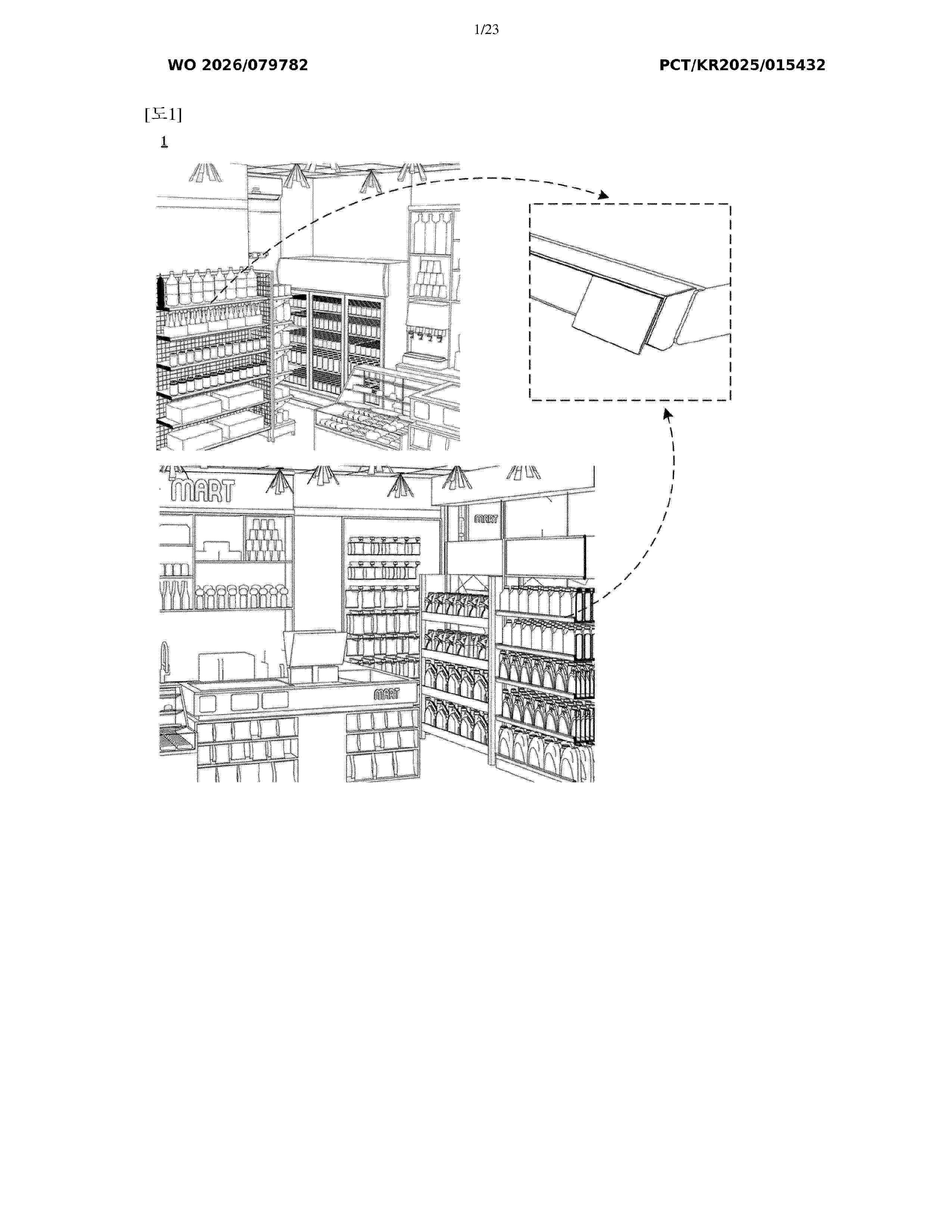
Resumen de: WO2026079782A1
An embodiment can provide a power rail for an electronic shelf label, comprising: a rail body part having a front surface to which an electronic display device is fastened, and having a rear surface fastened to a shelf; a first accommodation groove which is formed in the longitudinal direction of the rail body part and in which an additional device is accommodated; a second accommodation groove positioned below the first accommodation groove, and formed in the longitudinal direction of the rail body part; an electrode part provided in the second accommodation groove so as to supply power or data to the electronic display device; an array part provided in the second accommodation groove so as to fix the electronic display device; a first fastening-latch part formed on the rear surface of the rail body part and fastened to the shelf; and a second fastening-latch part formed on the front surface of the rail body part so that the electronic display device is provided thereon, wherein a portion of the electronic display device is inserted into the second accommodation groove so as to be electrically connected to the electrode part, and is fixed by means of the array part.
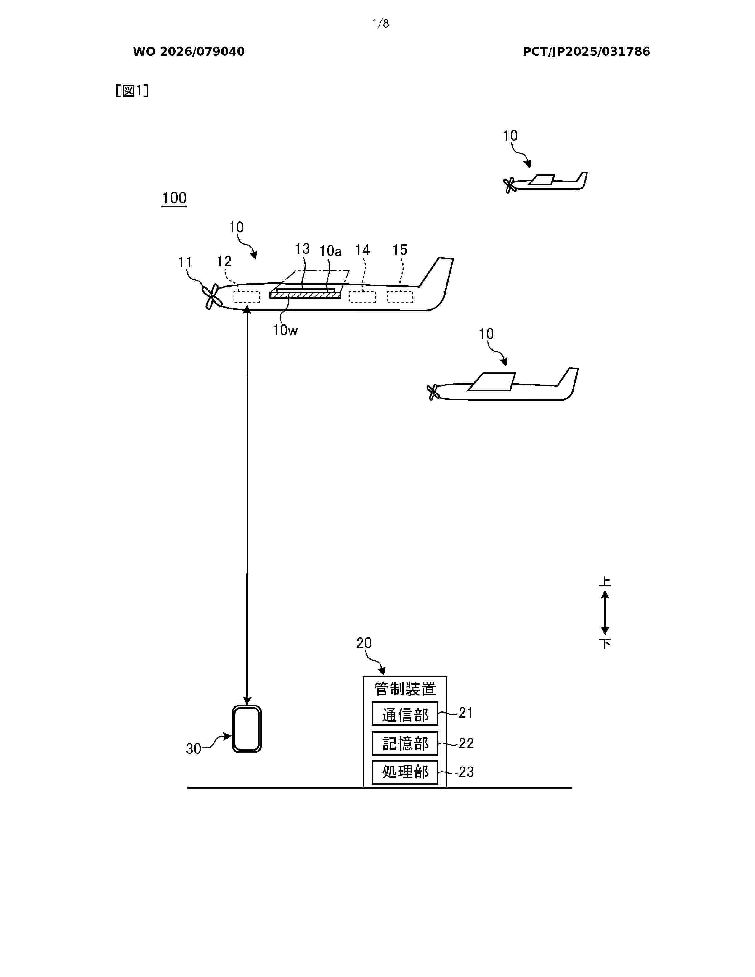
Resumen de: WO2026079040A1
This high-altitude platform system comprises a plurality of solar planes, each equipped with a communication platform, a solar cell mounted to at least an upper surface of a plane body, and an electricity storage device that stores electricity converted by the solar cell. The plurality of solar planes fly in a circular path, including a first area in which an electricity generation amount generated by the solar cell exceeds an electricity consumption amount consumed by the solar plane in a reference flight period and a second area in which the electricity generation amount is less than the electricity consumption amount in the reference flight period, such that a state in which a stored electricity amount stored in the electricity storage device is greater than 0 is maintained. In a period in which any one of the plurality of solar planes flies in the first area, another solar plane flies in the second area.
Resumen de: WO2026080923A1
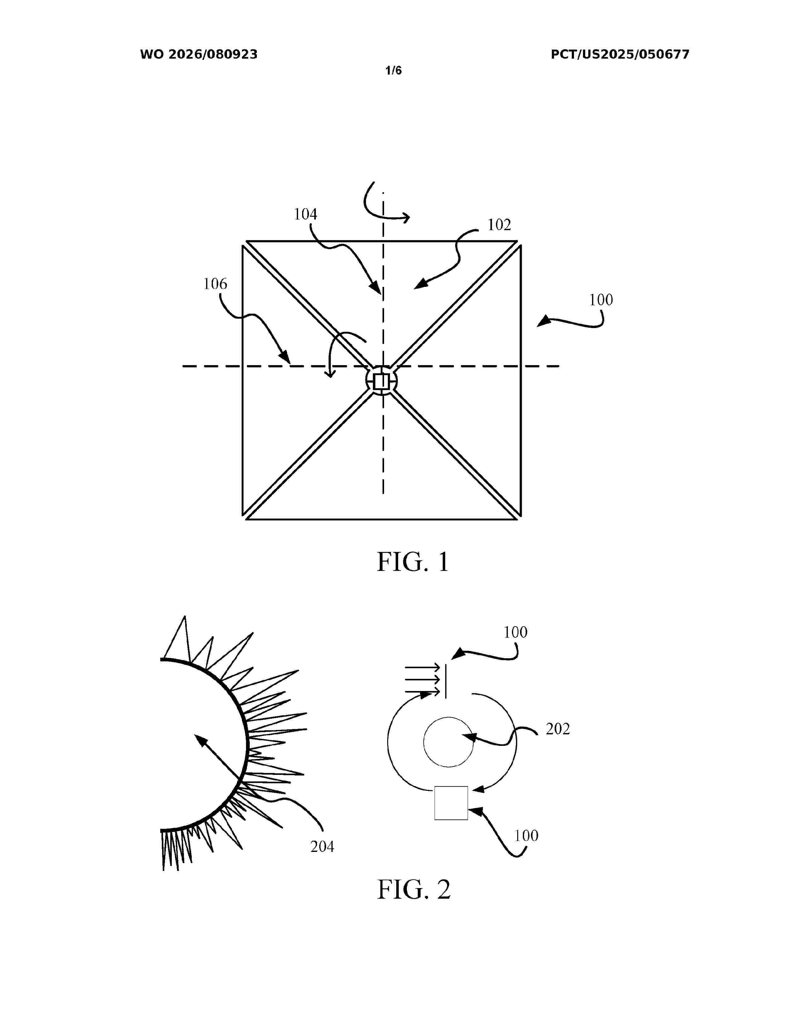
Systems and methods described herein include control systems and methods for solar sails. Control systems may include shape memory structures configured to position a solar vane when the shape memory structure changes temperature to a transition temperature. The control system may optionally include a biasing element in order to define the position and/or control of the solar vane during the movement of the vane when the shape memory structure is in the transition temperature.
Resumen de: US20260104446A1
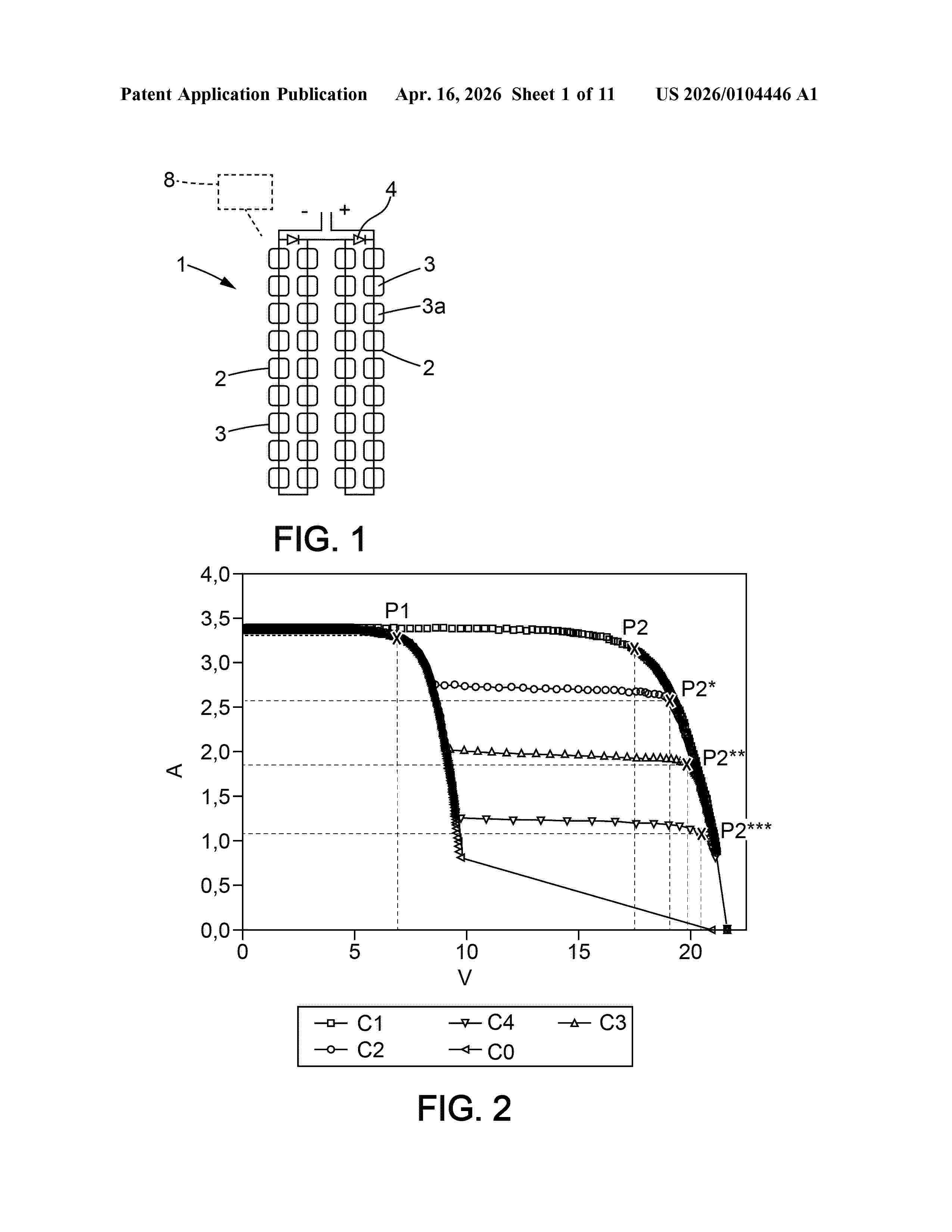
A method for testing at least one bypass diode in a photovoltaic system including at least one photovoltaic module that is in operation, the photovoltaic module includes at least one string of photovoltaic cells that are connected to a bypass diode dedicated to this string, the method includes: shading a portion of the cells of the string so as to cause a switch to bypass mode through the diode, this switch causing an increase in the temperature of the diode if the diode is in an operational state; measuring at least one temperature of the diode; and comparing the measured temperature with a threshold in order to deduce a state of the diode.
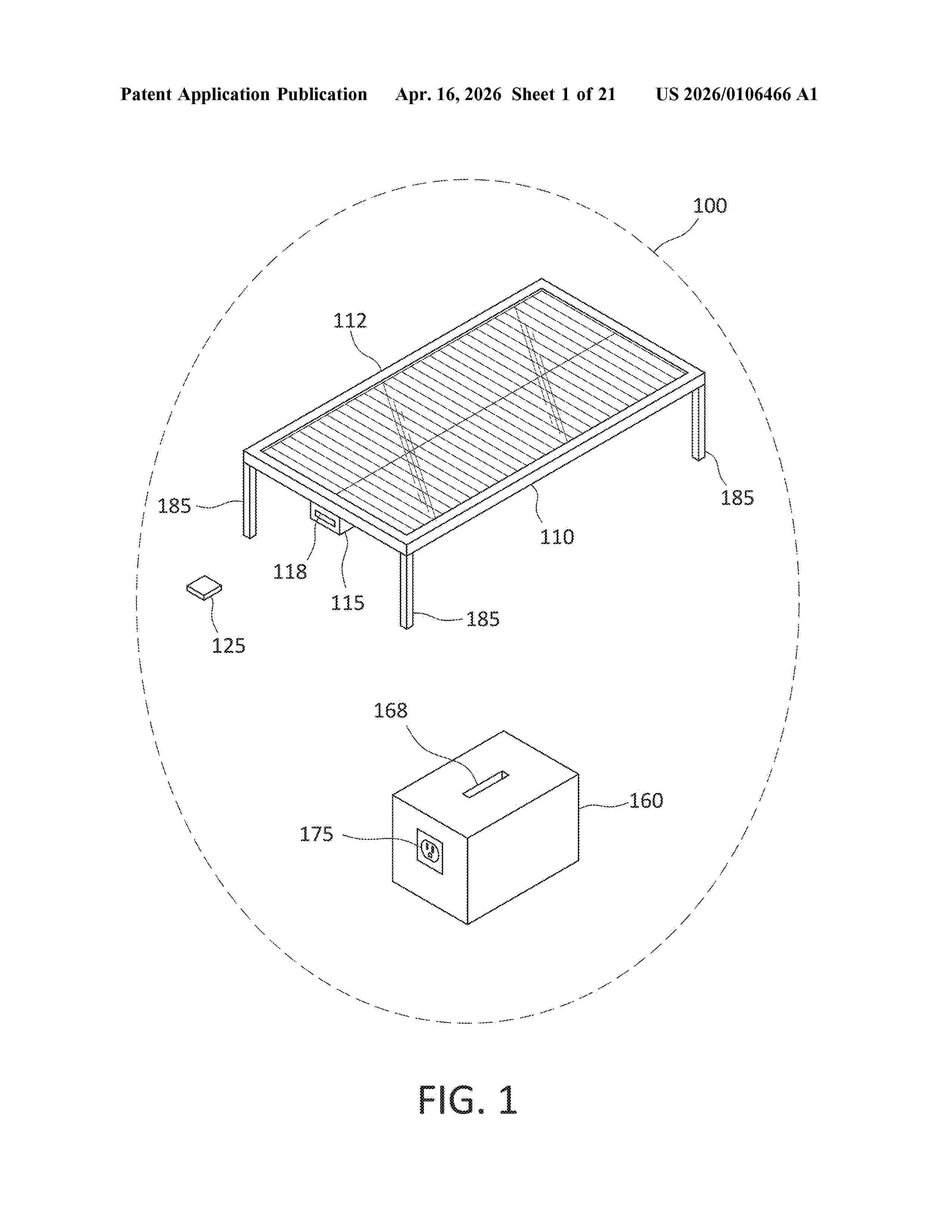
Resumen de: US20260106466A1
A system for utilizing renewable energy includes a rechargeable battery adapted to store energy, a solar panel device, and an inverter device. The solar panel device includes a solar panel adapted to receive sunlight and generate energy and a battery charger coupled to the solar panel. The battery charger is adapted to receive energy from the solar panel and store energy in the rechargeable battery. The inverter device includes a power outlet and is adapted to receive energy from the rechargeable battery and produce an electric current via the power outlet.
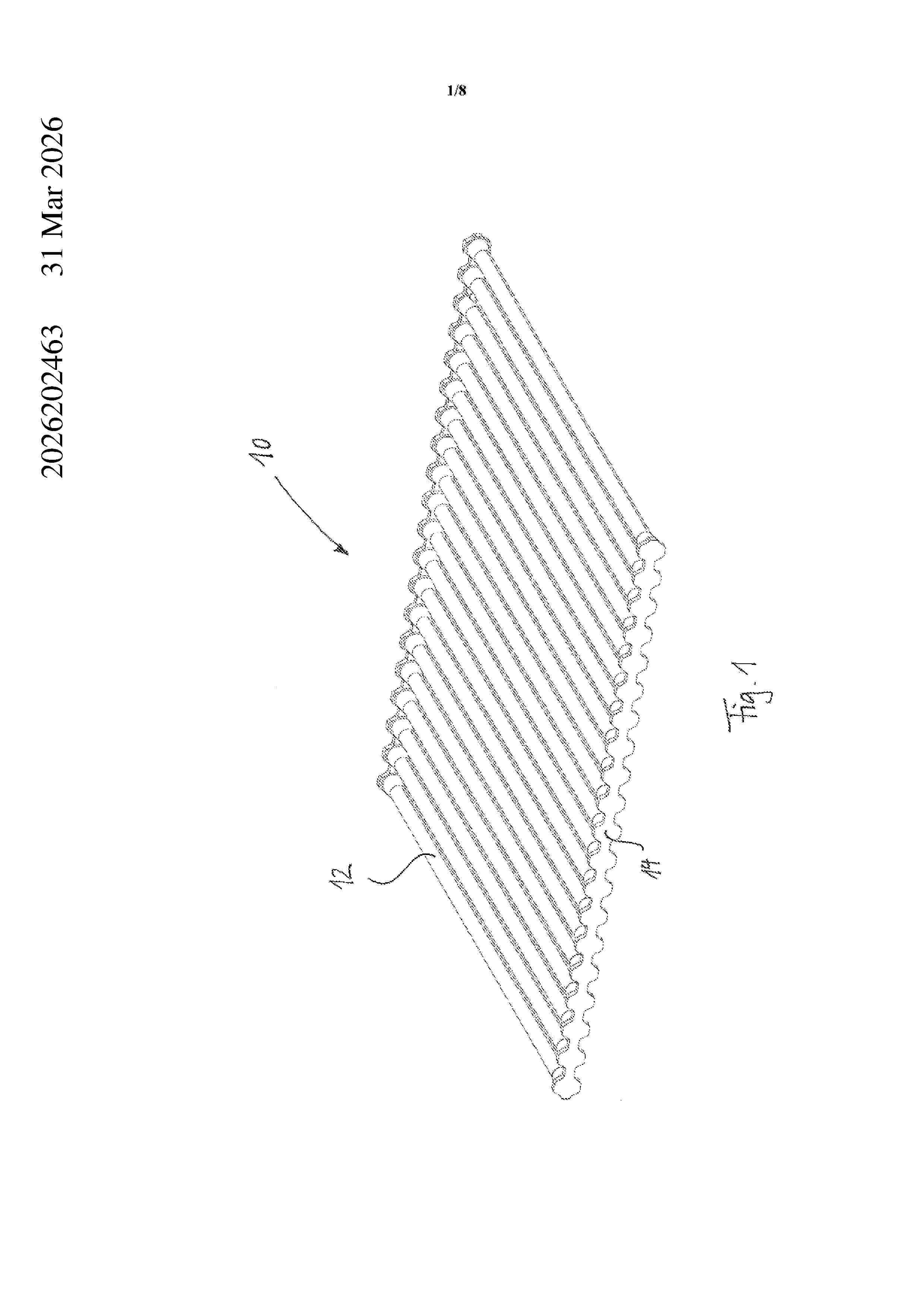
Nº publicación: AU2026202463A1 16/04/2026
Solicitante:
TUBESOLAR AG
Resumen de: AU2026202463A1
22561410_1 (GHMatters) P124631.AU.1 Abstract The present invention relates to a photovoltaic module (12), in which highly durable, integrally bonded sealing of the interior (18) of the tube (16) is ensured. The photo- voltaic module (12) is easy and cost-effective to produce and the efficiency of the photovoltaic module (12) in relation to the effective area for energy conversion is not compromised or is only negligibly compromised. The photovoltaic module (12) ac- cording to the invention is very low-maintenance and has a long service life. Further- more, the photovoltaic module (12) can be arranged with respect to a plurality of photovoltaic modules (12) arranged in parallel and can form a solar module formed for example from 20 photovoltaic modules (12). (Fig. 2) Abstract ar b s t r a c t a r 24a ( | 246 Fig 2 ar a r
 BOPI
BOPI
 Sede Electrónica