Si deseas distinguir tus productos, servicios o ambos de los de otra empresa, es posible que necesites una marca o nombre comercial. Descubre qué son, en qué consiste su procedimiento de registro y qué implica.

Información sobre los plazos de presentación de solicitudes de transformación de marcas de la Unión Europea en marca nacional española. Más información


Si tienes un nuevo dispositivo, producto o procedimiento que resuelva un problema técnico o tenga una ventaja práctica, existen distintas formas de protegerlo en España y en otros países. Descubre cómo hacerlo.

¿Tu innovación reside en la estética, la ornamentación o la apariencia de tu producto? Protégela mediante un diseño industrial. Descubre qué derechos confiere el registro y cómo realizar la tramitación.

Las patentes publicadas en todo el mundo son una valiosa fuente de información científica, técnica y comercial.
reembolso del 75% del coste de Búsquedas e Informes Tecnológicos de Patentes. Más información*

Si eres emprendedor/a o una empresa y quieres potenciar y mejorar la rentabilidad de tu negocio protegiendo de forma adecuada los activos intangibles de tu organización, en este espacio encontrarás lo necesario.


 226
resultados
226
resultados
 Última actualización
31/08/2024 [07:27:00]
Última actualización
31/08/2024 [07:27:00]


 Resultados 25 a 50 de 226

Resumen de: US2024290898A1
An adjustable electromagnetic energy converter comprises a body of transparent insulating material, a plurality of stacked identical electromagnetic energy converting cells, and a heat transfer system. Methods are herein provided for determining a configuration to which to adjust the converter and optimizing its performance. The methods comprise first determining electrical outputs of a first and a second configuration of the converter, comparing the electrical outputs, and determining whether to adjust the converter from the first configuration to the second configuration. To optimize the performance of the converter, the following configuration characteristics can be adjusted: electromagnetic energy collection area or orientation of the body of transparent insulating material, angle between adjacent cells, angle between the cells relative to the incoming electromagnetic energy, or spacing between adjacent cells.

Resumen de: US2024290905A1
A solar cell includes a silicon substrate, a first doped region, and a second doped region. The first doped region includes a first passivated contact region on the silicon substrate and a second passivated contact region on the first passivated contact region. The first passivated contact region includes a first doped layer, a first passivation layer, and a second doped layer. The second passivated contact region includes a second passivation layer and a third doped layer. The second doped region includes a third passivation layer. Each of the first and third passivation layers includes a porous structure. One of the first and second doped regions is a P-type doped region, the other of the first and second doped regions is an N-type doped region, and a hole density of a corresponding passivation layer in the P-type doped region is greater than that in the N-type doped region.
Resumen de: US2024290899A1
The invention relates to a solar module with improved bonding. The solar module (100) comprises a front encapsulant layer (104), solar cells (106), a middle encapsulant layer (108), a back contact foil (210b) with a patterned copper pattern (210b) thereon, and a back encapsulant layer (112). Inventors found that, when producing such a solar module, the bonding between the middle encapsulant layer and the copper side of the back contact foil was insufficient. A solution is found in providing cut-outs in the back contact foil through which the back encapsulant layer can bond to the middle encapsulant layer and/or the solar cells.
Resumen de: WO2024175154A1
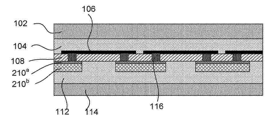
The invention relates to a method for improving the contact resistance of a multi-solar cell (1) comprising a front face (100), a rear face (101), and multiple sub-cells (2.3). The method has the steps of: a) providing (31) the multi-solar cell (1) with a front-face contact (11) and a rear-face contact (25), said front-face contact (11) and/or rear-face contact (25) having a grid-shaped, strip-shaped, or transparent design, b) electrically contacting (32) a region of the rear-face contact (25) with a contacting device (4) which is electrically connected to one pole of a voltage source (9) and contacting the front-face contact (11) or another region of the rear-face contact (25) which is electrically insulated from the aforementioned region with another contacting device (4) which is electrically connected to the other pole of the voltage source (9), c) applying (33) a voltage, which is oriented opposite the forward direction of the multi-solar cell (1), to the front-face contact (11) and the rear-face contact (25) by means of the voltage source (9), the value of the applied voltage being lower than the breakthrough voltage of the multi-solar cell (1), and d) guiding (34) at least one point light source (5) over the front face (100) and/or the rear face (101) of the multi-solar cell (1) while the voltage is being applied, wherein in the process, one or more sections (6) of a sub-region of the front or rear face (100, 101) are illuminated so that a flow of current is induced in
Resumen de: WO2024175153A1
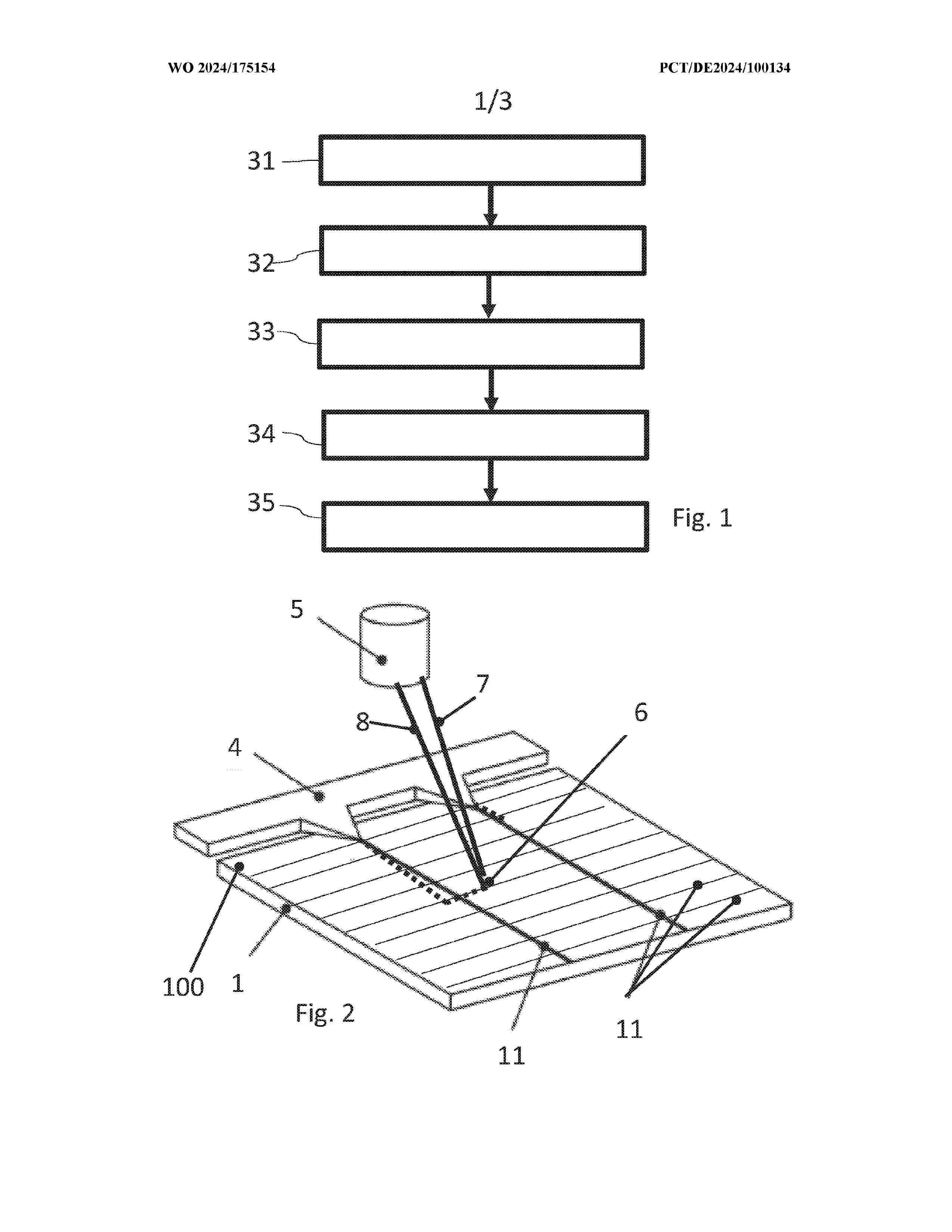
The invention relates to an apparatus for improving the ohmic contact between a front-side contact (14) and a doped layer of a wafer solar cell (1), the wafer solar cell (1) comprising: a front side (11), a rear side (12), the front-side contact (14), the doped layer, and a rear-side contact (15), the front-side contact (14) and the rear-side contact (15) having a strip-shaped or grid-shaped design. The apparatus comprises: - two contacting devices (6) for electrically contacting the front-side contact (14) and the rear-side contact (15); - a voltage source (7) having one pole for electrical connection to one contacting device (6) and a further pole for electrical connection to the other contacting device (6); - two point light sources (4), one point light source (4) being configured and designed to illuminate the front side (11), and the other point light source (4) being configured and designed to illuminate the rear side (12). The contacting devices (6) each have: • an optically transparent material which is coated with an optically transparent, electrically conductive layer; • an optically transparent material (62) having a plurality of microscopically thin, electrically conductive wires (61) which are integrated into a surface of the optically transparent material (62); • an optically transparent, electrically conductive material having a plurality of microscopically thin, electrically conductive wires which are integrated into a surface of the optically transparen
Resumen de: US2024290896A1
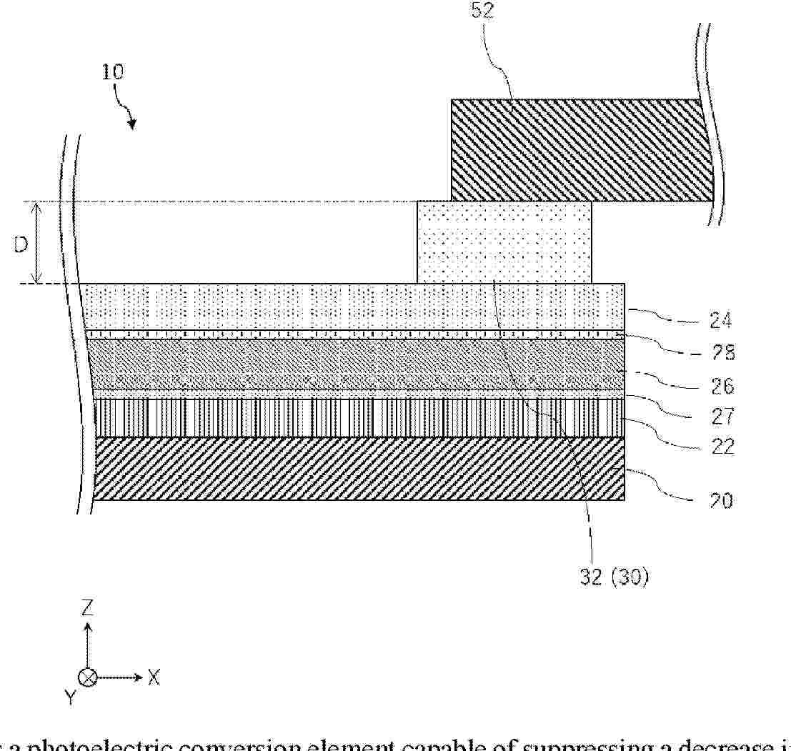
Provided is a photoelectric conversion element capable of suppressing a decrease in strength. A photoelectric conversion element comprises: a photoelectric conversion layer (26); an electrode layer (24) adjacent to the photoelectric conversion layer; a collecting electrode (30) adjacent to the electrode layer; and a conductor (50) joined to the collecting electrode. The thickness of the collecting electrode (30) at least at a joint portion between the collecting electrode (30) and the conductor (50) is 4 μm or more.
Resumen de: US2024290895A1
The invention discloses an electrode paste in contact with a p+ emitter of an N-type solar cell, and relates to the technical field of photovoltaic cells. The electrode paste of the present invention comprises the following components by weight: 80-90 parts of a conductive silver powder, 0.5-3 parts of an aluminum powder, 3-8 parts of a glass powder, 0.1-2 parts of a lanthanum-aluminum alloy powder or lanthanum-ytterbium-aluminum alloy powder, 6-10 parts of an organic vehicle and 0-2 parts of an auxiliary agent. By selecting the components and formulations of the electrode paste, the electrode pastes of present invention obtained improve the conversion efficiency of a N-type solar cell that can exceed 23.5% after the electrode paste being applied to the N-type solar cell.
Resumen de: DE102023104920A1
Es werden eine Messvorrichtung (1) und ein Verfahren zum Bestimmen einer spektralen Bestrahlungsstärkeempfindlichkeit SR(λ) (17) und eines spannungsabhängigen Stromverhaltens /(U) unter Standard-Sonne-Bedingungen einer Photovoltaikeinheit (3) beschrieben. Die Messvorrichtung umfasst eine Beleuchtungsquelle (5), eine Kontaktierungseinrichtung (7), eine Steuerung (9) und eine Auswerteeinrichtung (11). Die Beleuchtungsquelle kann wahlweise Licht (13) mit variierbaren Spektralverteilungen (15) oder mit einem standardisierten Sonnenspektrum emittieren. Die Steuerung kann in einem ersten Betriebsmodus die Beleuchtungsquelle zur Emission des Sonnenspektrums und in einem zweiten Betriebsmodus zur sukzessiven Emission von Licht mit einer Vielzahl N verschiedener Spektralverteilungen ansteuern. Die Auswerteeinrichtung ist dazu konfiguriert, in dem ersten Betriebsmodus aus einem gemessenen PV-Strom Imeasdas spannungsabhängige Stromverhalten I(U) der Photovoltaikeinheit (3) unter Einwirkung des standardisierten Sonnenspektrums zu bestimmen und in dem zweiten Betriebsmodus aus mehreren bei Beleuchtung mit den N verschiedenen Spektralverteilungen (15) jeweils gemessenen Strömen Imeas,n(n = 1...N) und unter Berücksichtigung einer für jede der N Spektralverteilungen vorbekannten spektralen Bestrahlungsstärke Eλ,n(λ) (n = 1...N) die spektrale Bestrahlungsstärkeempfindlichkeit SR(λ) der Photovoltaikeinheit zu bestimmen.
Resumen de: WO2024176193A1
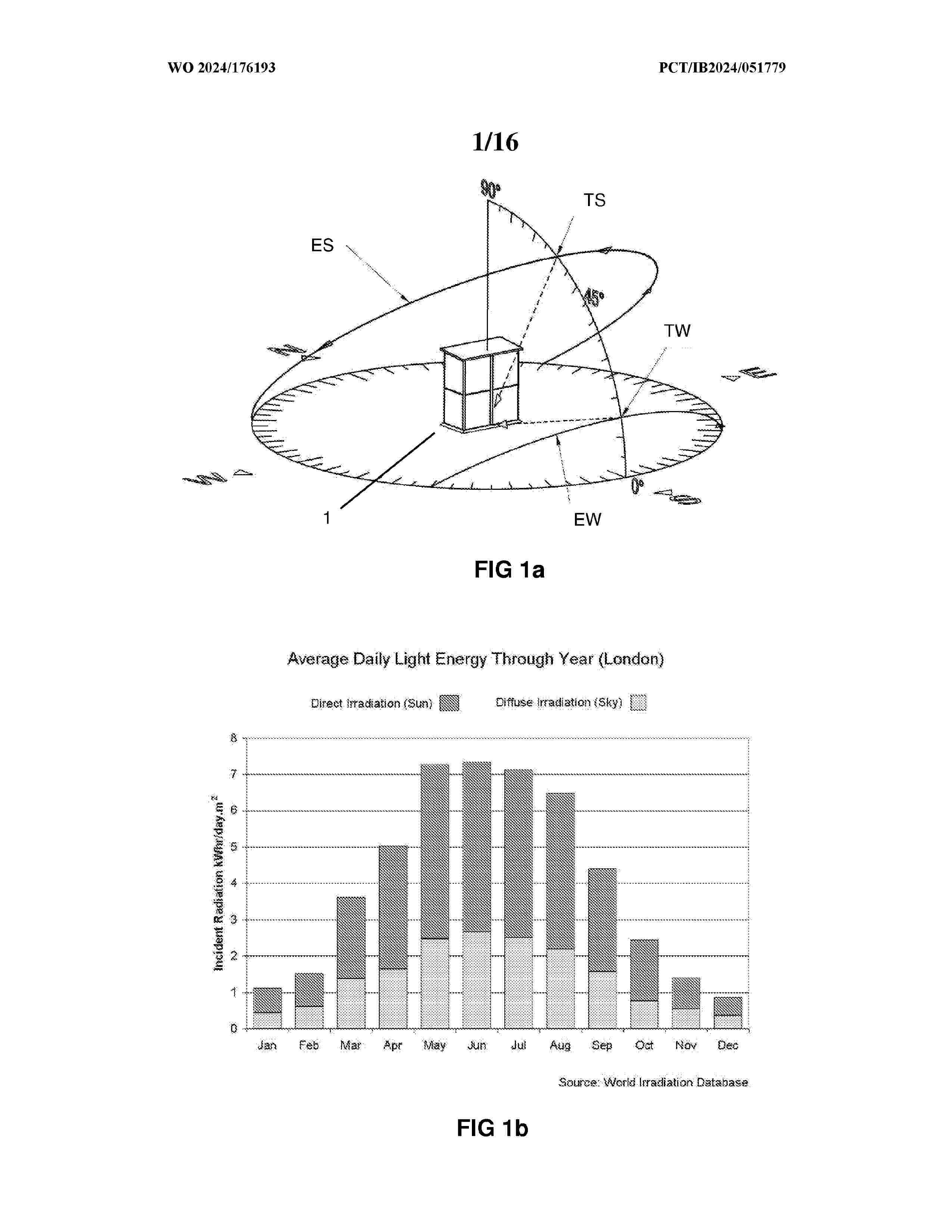
A charging station comprising a structure or enclosure for charging batteries of an EV vehicle whether said batteries are removed from an EV for a charging cycle or where the EV is coupling directly to charging point. The invention provides for the accommodation or storage of electric vehicles (EVs) or batteries used therein to facilitate charging thereof via means for charging battery cells of an electric vehicle (EV) utilising power predominantly derived from solar radiation via photovoltaic panels or PV arrays. Embodiments include charging stations for electric vehicles (EVs), particularly bikes and scooters. There is further described methods of forming a charging station having multiple access doors through which batteries for an EV or an EV can be coupled to a charging port. In a preferred construction, a standalone charging station for EV scooters provides means for mounting and storing the scooters during a charging cycle. A municipal scooter hiring system is also disclosed.
Resumen de: WO2024176191A1
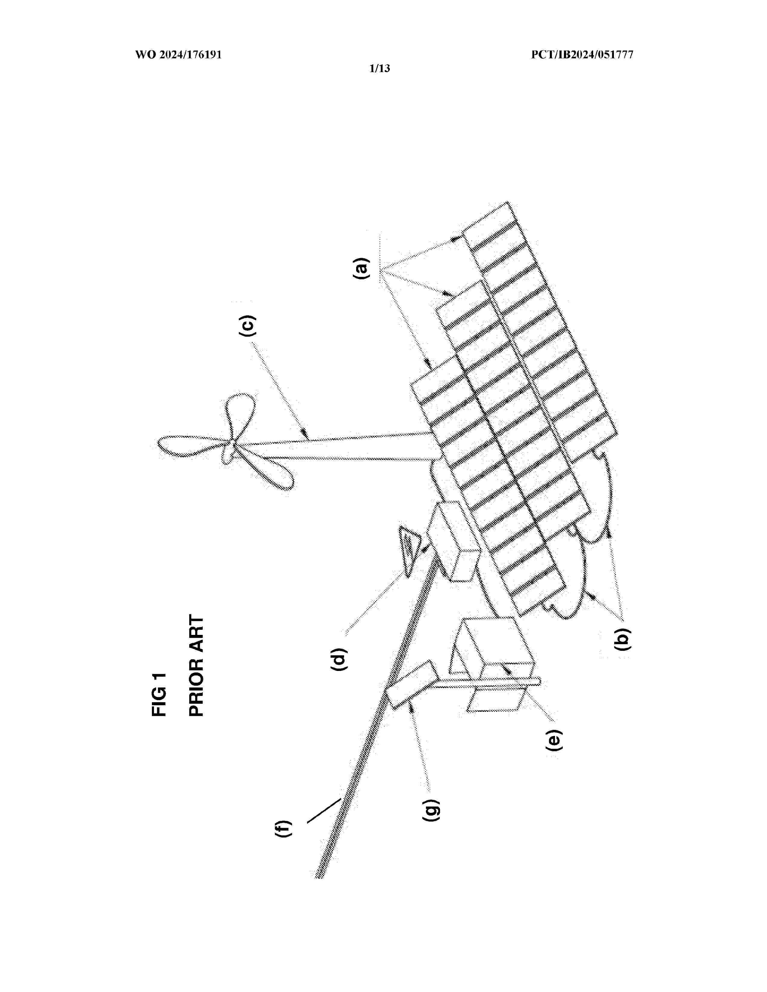
The invention describes a photovoltaic (PV) power generator ideally suited for off- grid and remoted locations having a substantially upright structure and comprising an enclosure, adapted to be ground-engaging, upon which there is mounted a plurality of vertically disposed PV panels. The enclosure houses control circuitry for the harvesting, storage and delivery of electrical energy generated via the PV panels. Excess energy is accumulated in battery packs and delivered upon demand when supply via the PV panels is insufficient. The generator is optimised to a power rating ideal for off-grid living (average daily output of 200Wh/day) and for sustaining a domestic dwelling during seasonal minima of solar radiation and is provided with sufficient PV energy harvesting area to deliver the average daily rated output.
Resumen de: WO2024175989A1
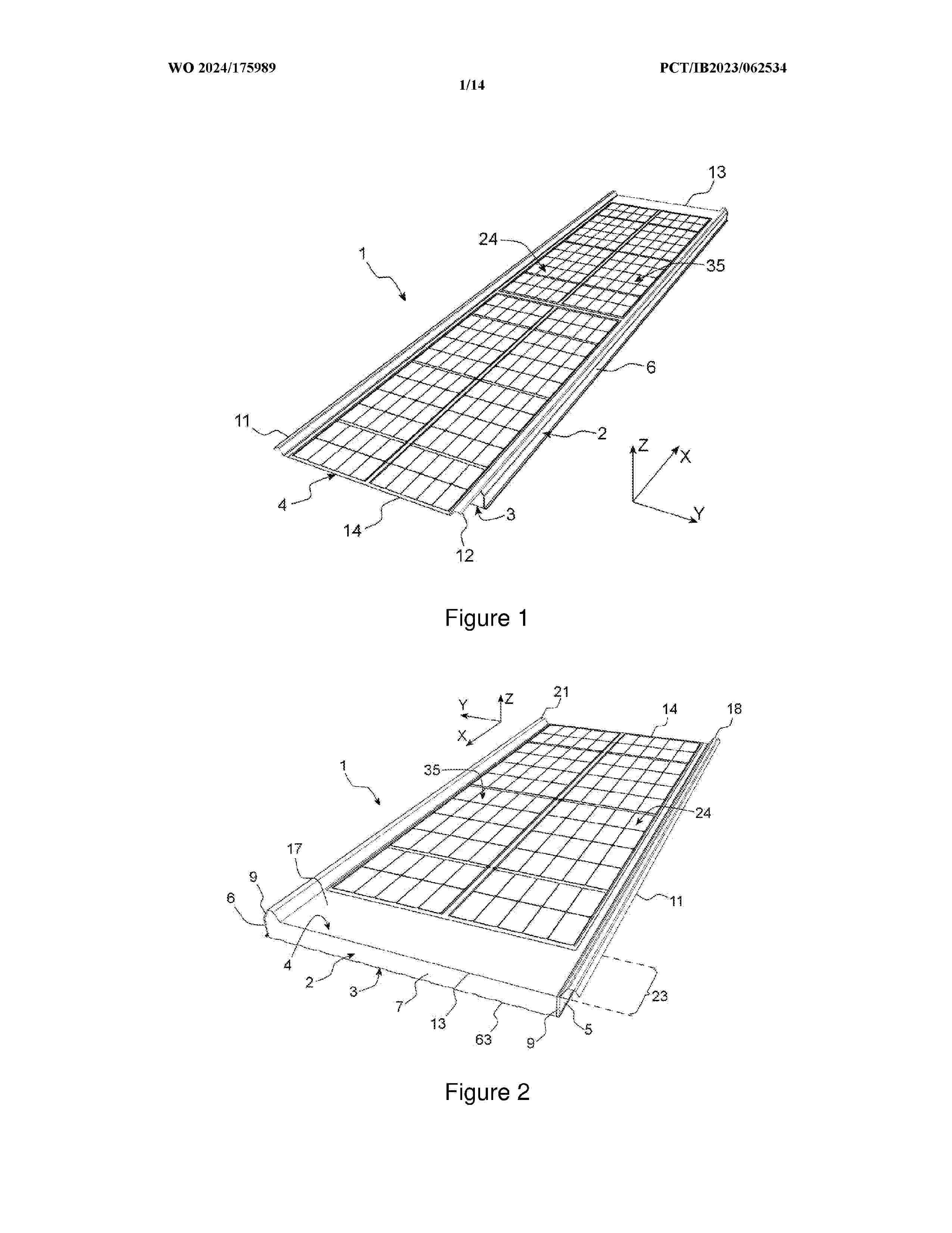
The invention relates to a sandwich panel (19 comprising a photovoltaic active area (24) positioned on the outer sheet (4) and whose upper, respectively lower, electrical connector is positioned in an upper, respectively lower, cavity (44, 45), the upper cavity being positioned within the insulation material (2) in the upper half of the sandwich panel and adjacent to either the second longitudinal side of the insulation material or the inner sheet so that the upper electrical connector can be accessed from the upper cavity, the lower cavity being positioned within the insulation material in the lower half of the sandwich panel and adjacent to either the second longitudinal side of the insulation material or the inner sheet so that the first lower electrical connector can be accessed from the lower cavity.
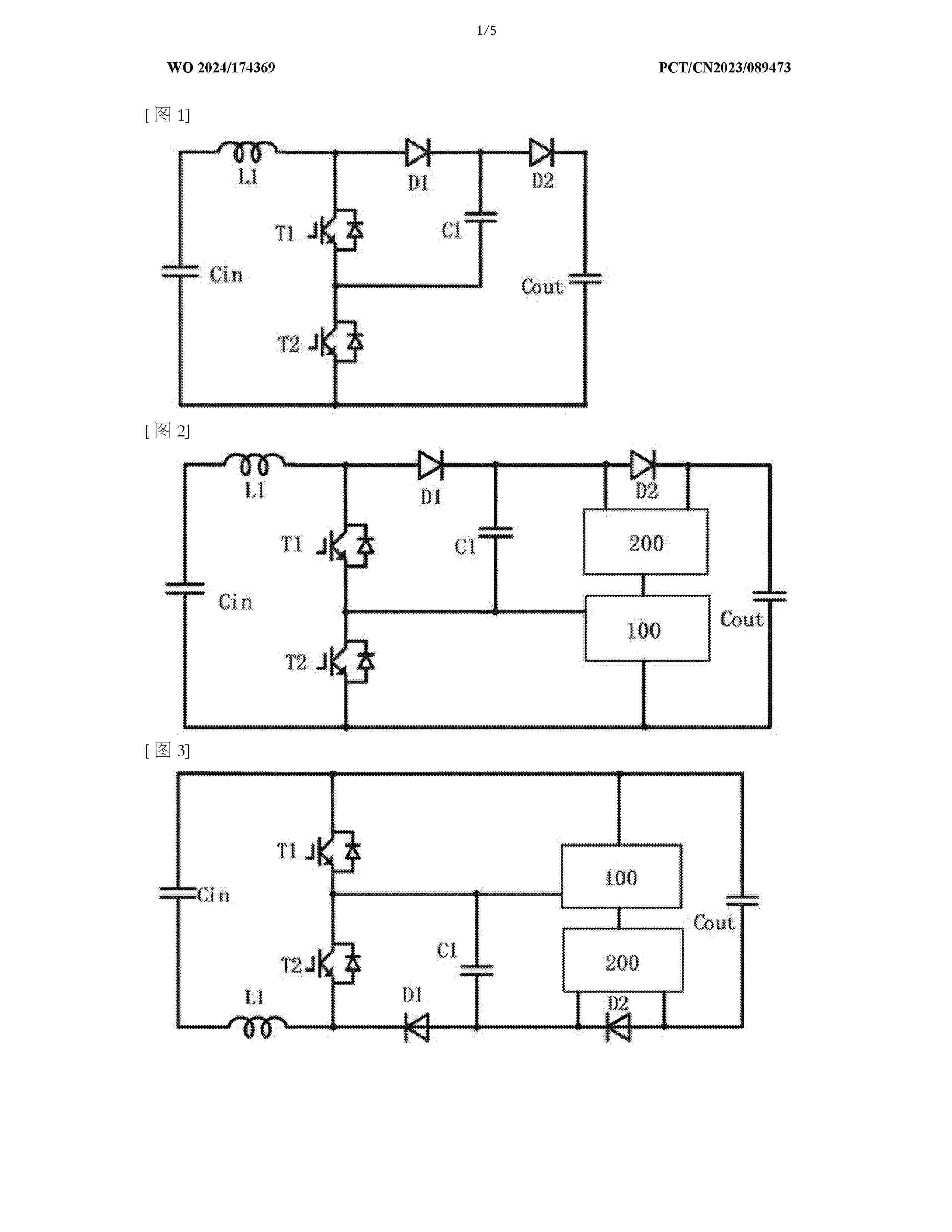
Resumen de: WO2024174369A1
The present application is applicable for the technical field of electronic circuits, and in particular, provides a boost circuit structure, an inversion device, and a photovoltaic power generation system. The structure comprises a switch circuit, a boost main circuit, a boost branch circuit, a first functional circuit, and a second functional circuit. According to the present application, a boost circuit structure frame is formed by the switch circuit, the boost main circuit, and the boost branch circuit, and the first functional circuit is connected to a flying capacitor and an input terminal II, so that the flying capacitor is charged in the power-on process of an input side of the boost circuit, and a second controllable switch is protected from overvoltage; and the second functional circuit is connected in parallel with a second diode, so that the flying capacitor is charged in the power-on process of an output side of the boost circuit, and the second diode is protected from overvoltage.
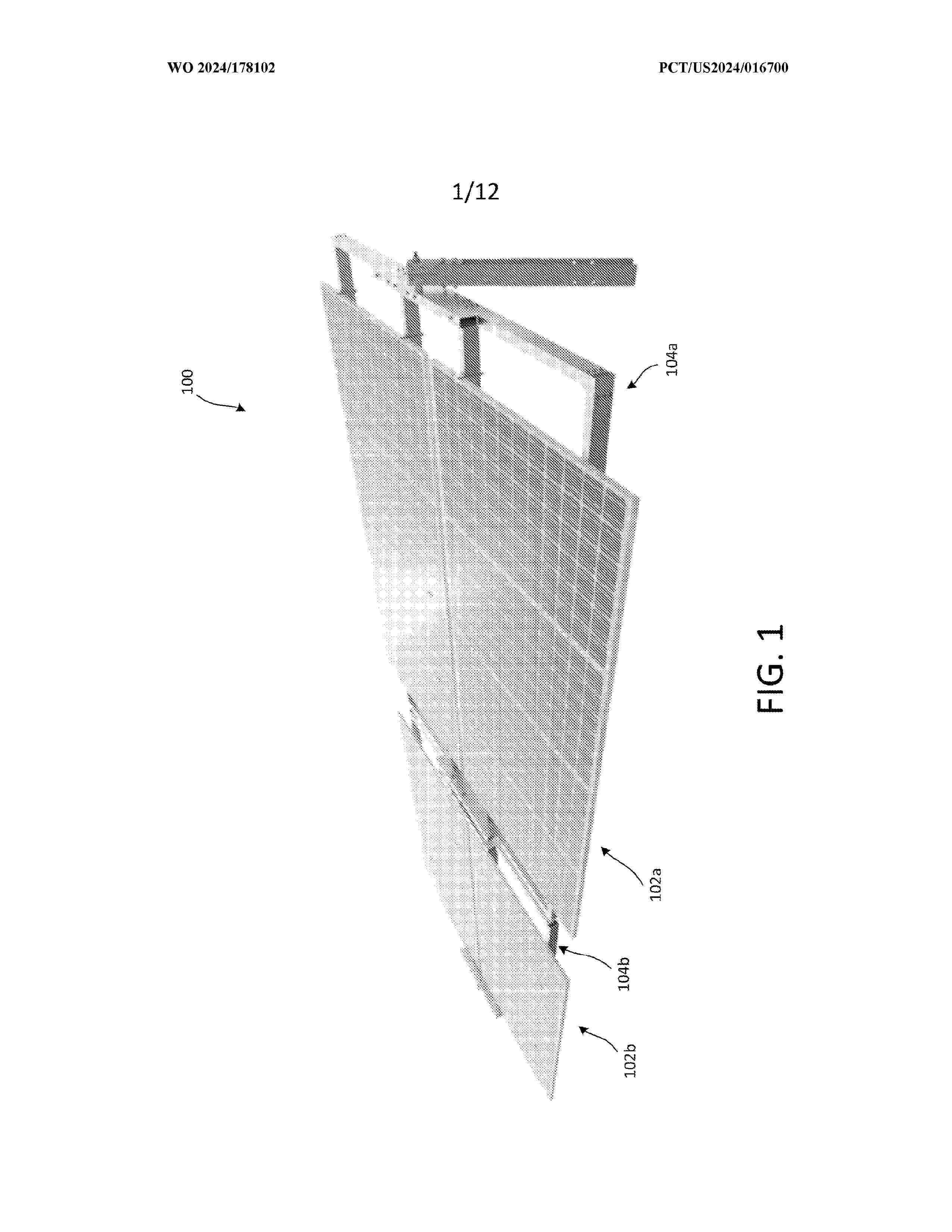
Resumen de: WO2024178102A1
A solar racking system for mitigating deformation and fatigue at critical joints and for providing increased clamping force between solar racking and solar panels is disclosed. The solar racking system includes one or more shock mount systems configured to reduce vibrations within the solar racking system, thereby preventing hole elongation and in turn, allowing the solar racking system to withstand critical wind events and other harsh weather conditions. Moreover, the solar racking system includes a dual clamp system having angled clamping plates and planar clamping plates configured to couple solar panels to racking of the solar system that provide increased clamping force, thereby providing maximum strength and vibration resistance.
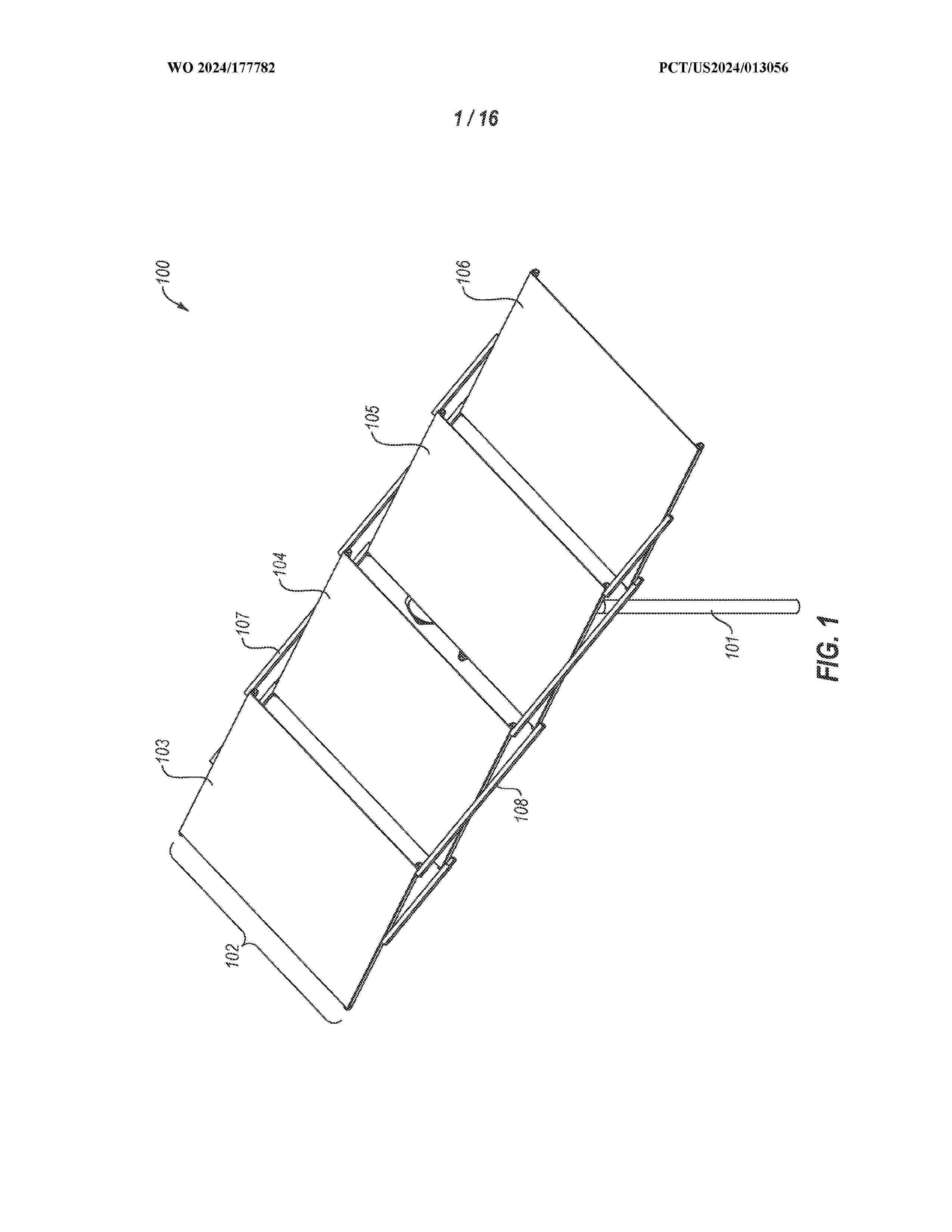
Resumen de: WO2024177782A1
A collapsable shading apparatus with panels. Embodiments of the present invention vary, but generally include: a post portion; a panel array having two or more panels (including solar) and that is pivotally connected to the post portion; and a scissor-arm assembly attached to and connecting the panels. The array is moveable towards any sun position in the sky. Some embodiments include a slider arm to support the array, while others do not. With the scissor-arm assembly, panels are configured to extend to a deployed position and stack in a collapsed position. In the deployed position, the panels are offset in depth with gaps in-between to reduce wind load on the array. Deployed panels are also substantially non-overlapping to minimize intra-panel shading and provide contiguous shade. Various embodiments collapse and disassemble to fit into a conveniently portable container.
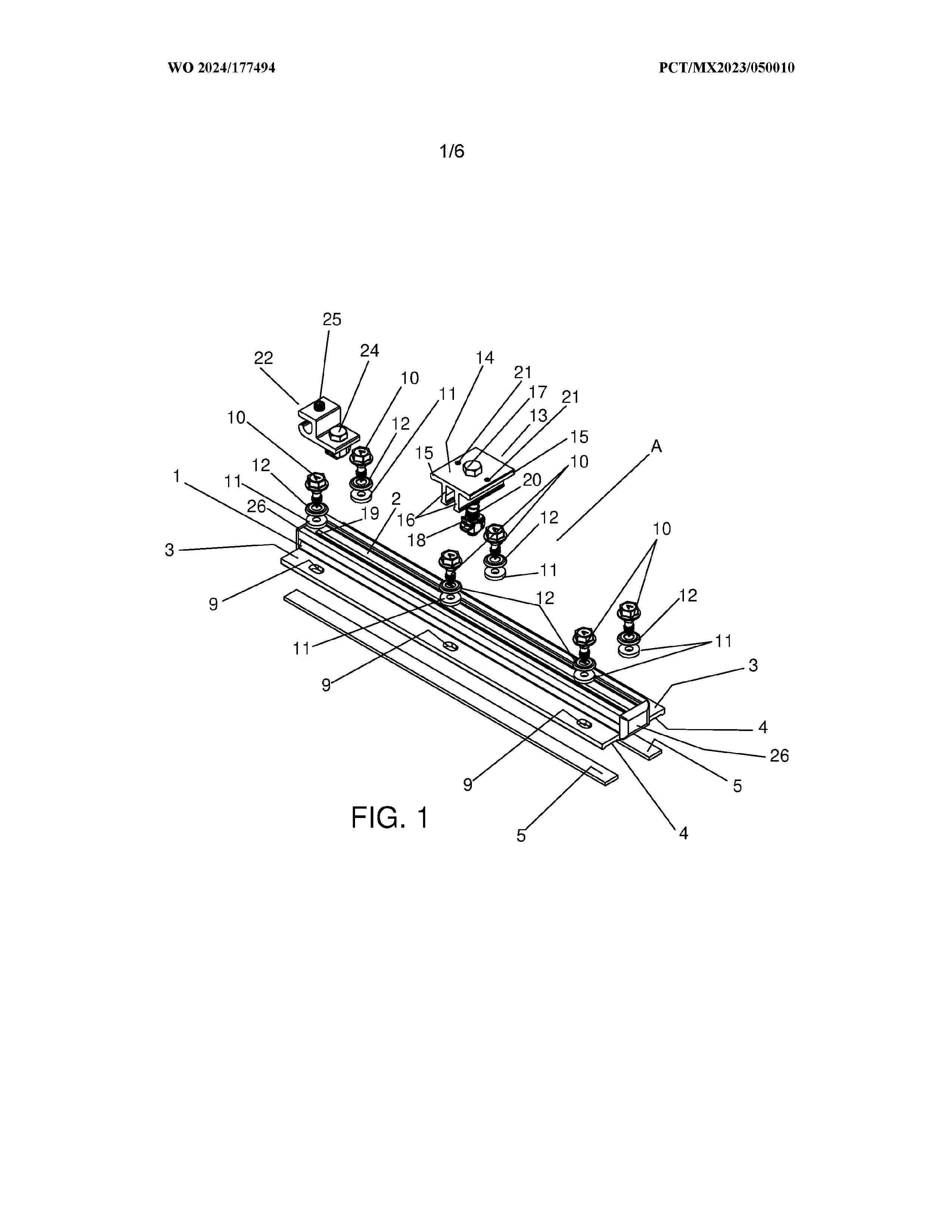
Resumen de: WO2024177494A1
The invention relates to a system for securing photovoltaic modules on trapezoidal sheet roofs, characterised by comprising modular units defined by a ribbed profile defining a longitudinal central channel on its upper face and two lateral protruding arms designed with a longitudinal recess or channel on its lower face to receive sealing insulating strips for creating an impermeable seal against the trapezoidal sheet where it is to be fixed and being preferably arranged on the ridge of the trapezoidal sheet roof; furthermore said lateral arms comprise through holes designed to receive securing means with sealing and gripping means to create a secure and impermeable fastening; wherein said longitudinal central channel of the upper face of the corrugated profile is designed to receive securing clips for securing the side edges of solar panels.
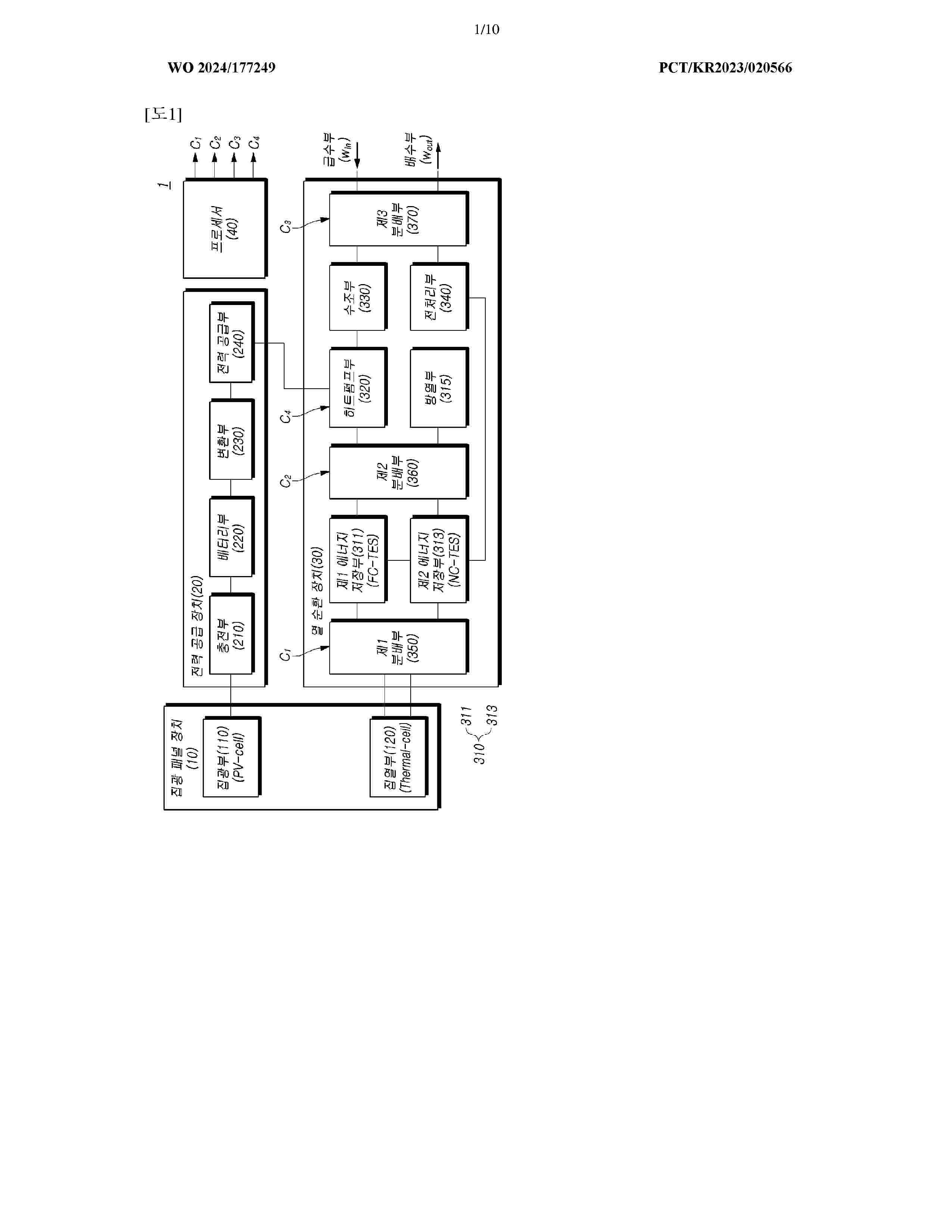
Resumen de: WO2024177249A1
One embodiment of the present disclosure relates to a photovoltaic thermal regeneration system for efficiently controlling the temperature of a light collection panel, and an operating method therefor. The system therefor may comprise: a light collection panel unit, which uses a refrigerant flowing in a pipe passing through the rear surface thereof, so as to absorb the heat generated from a photovoltaic (PV) cell arranged on the front thereof; and at least two energy storage units which have an inner space filled with a thermal energy storage material, and which transfer the heat to the thermal energy storage material from the thermal energy of the refrigerant absorbing the heat while passing through the light collection panel unit, and then flowing through the pipe passing through the inner space. Other various embodiments are possible.
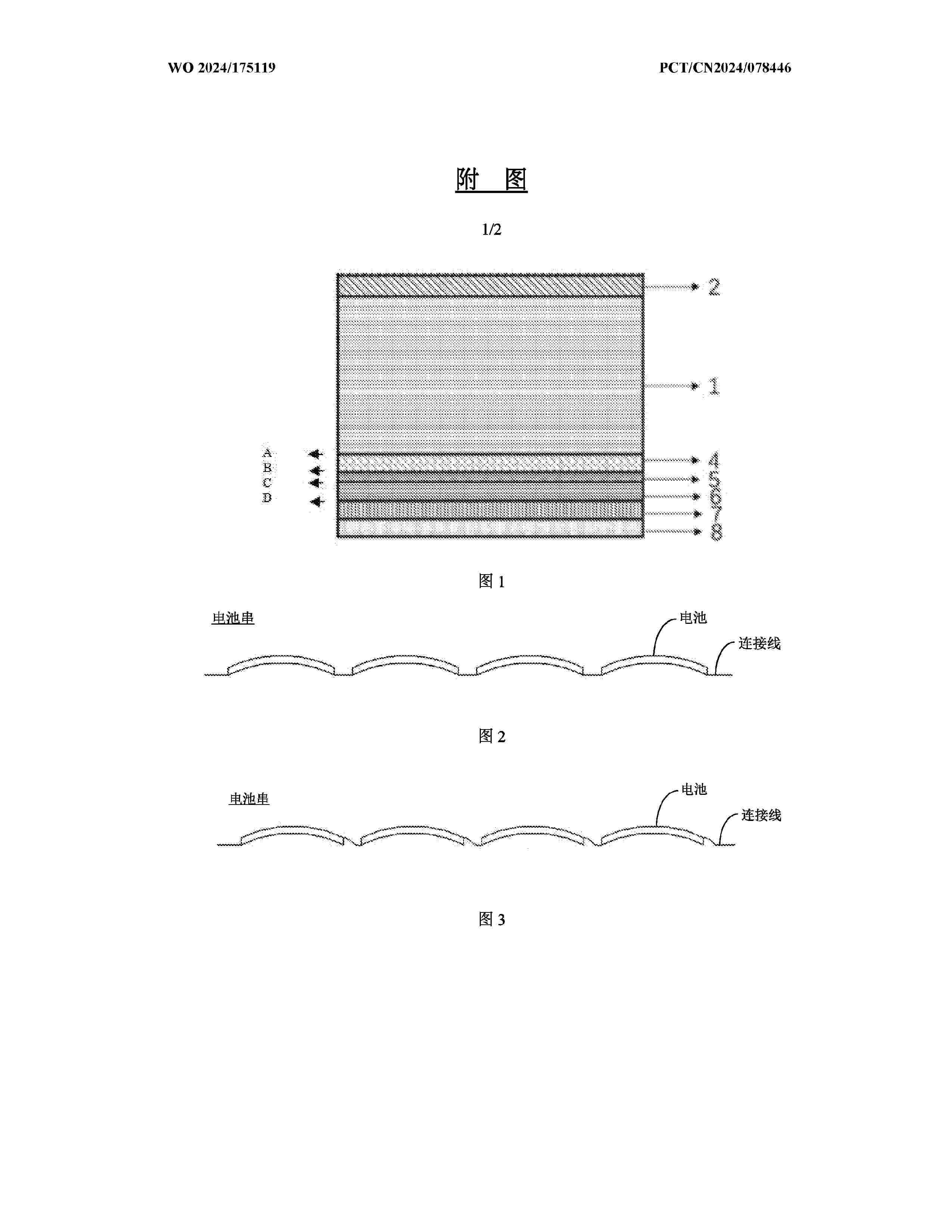
Resumen de: WO2024175119A1
The present application relates to a silicon wafer, the concentration of antimony in the silicon wafer being 4E+14cm-3 to 2E+16cm-3, and the total oxygen content of the silicon wafer being 25 ppma or less, preferably 18 ppma or less, and further preferably 14 ppma or less. The present application relates to a cell and a cell module comprising the silicon wafer. The present application relates to a cell, a substrate of the cell comprising antimony, the concentration of antimony being 4E+14cm-3 to 2E+16cm-3, preferably 4.30E+14cm-3 to 1.9E+16cm-3, and further preferably 4.45E+14cm-3 to 1.87E+16cm-3, and the total oxygen content of the substrate being 35 ppma or less, preferably 25 ppma or less, and further preferably 18 ppma or less.
Resumen de: WO2024174928A1
Disclosed in the present application are a display assembly and an electronic device. The display assembly comprises a protective assembly and a flexible display screen, the protective assembly being attached to the flexible display screen, and the flexible display screen comprising a folding portion and a non-folding portion. The protective assembly comprises: a protective layer, a bonding layer, and a liquid filling layer; the protective layer is connected to the flexible display screen by means of the bonding layer; the bonding layer is provided with a through hole; the through hole is opposite to the folding portion; and the liquid filling layer is disposed in the through hole.
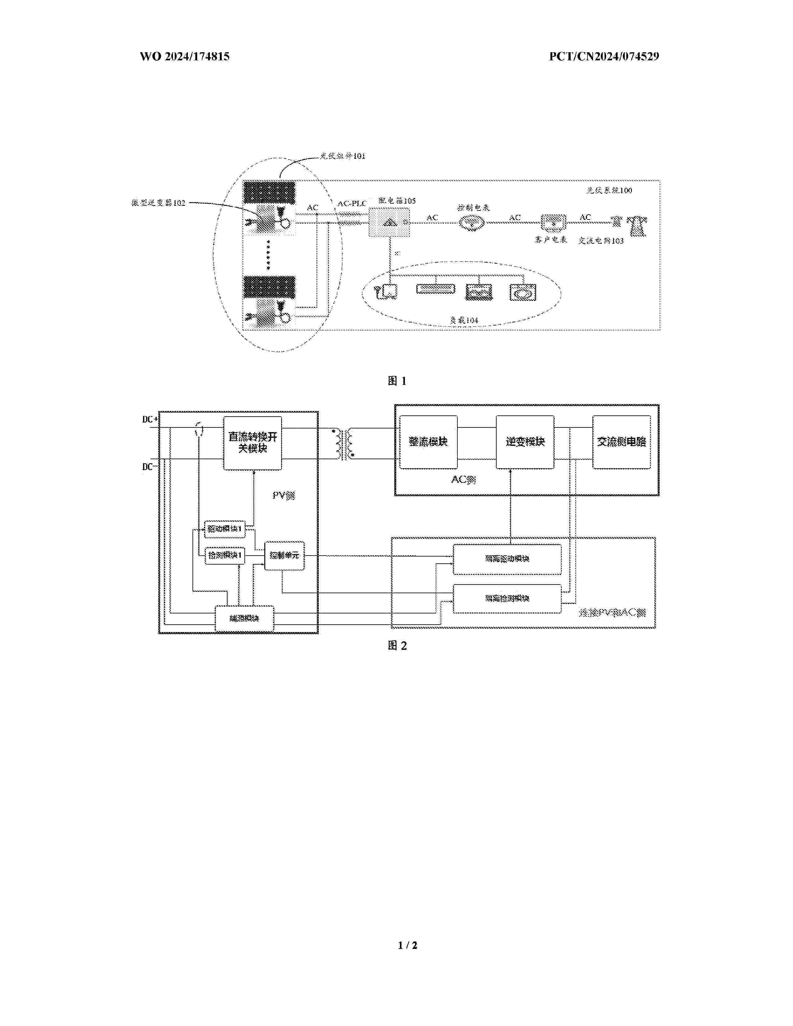
Resumen de: WO2024174815A1
Disclosed in the present application are a photovoltaic inverter and a photovoltaic system. The photovoltaic inverter comprises a photovoltaic side circuit, which is connected to a photovoltaic assembly, a transformer, and an alternating-current side circuit, wherein the photovoltaic side circuit comprises a direct-current conversion switching module and a first control module, which is connected to the direct-current conversion switching module; the first control module comprises a first control unit; the first control unit is used for controlling the direct-current conversion switching module to perform alternating processing on a first direct current, which is outputted by the photovoltaic assembly; the alternating-current side circuit comprises an inversion module and a second control module, which is connected to the inversion module; the second control module comprises a second control unit; and the second control unit is used for controlling the inversion module to perform inversion processing on a second direct current. Two control modules are used to respectively control a direct-current conversion switching module and an inversion module, such that requirements for an information processing capability of a single control module are reduced, and the use of an isolation driving circuit and an isolation detection circuit can be avoided, thereby reducing product cost.
Resumen de: WO2024174725A1
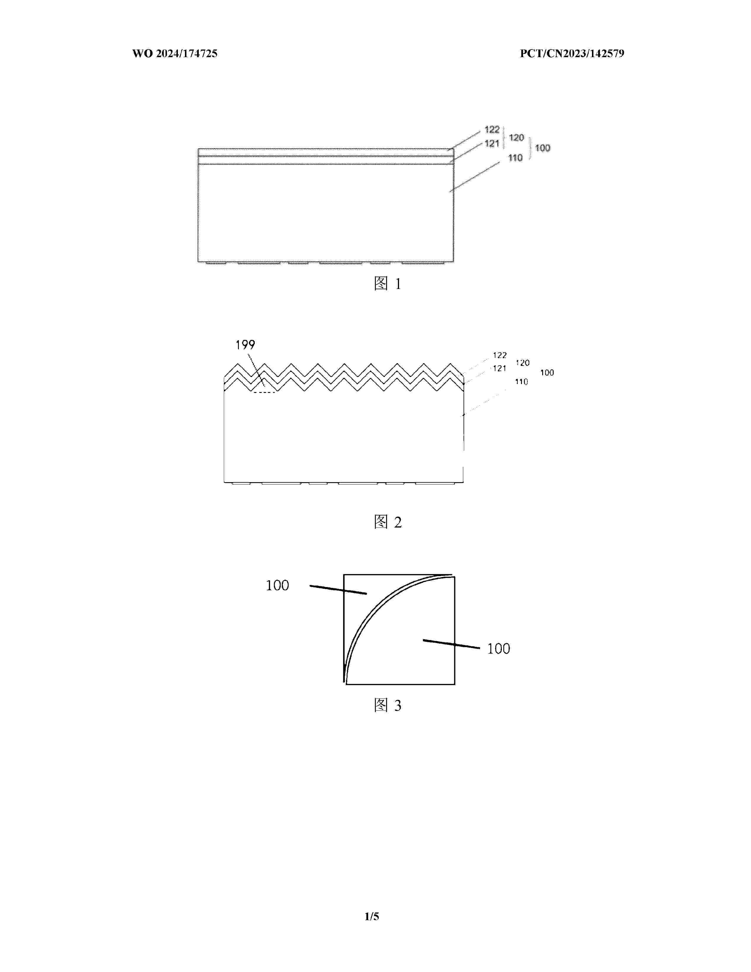
A photovoltaic cell, comprising a plurality of assembled cell pieces (100). Edges of the plurality of assembled cell pieces (100) are connected in an assembled manner. Each assembled cell piece (100) comprises a cell body (110), and a surface optical layer (120) located on a light-incident side of the cell body (110), wherein the surface optical layer (120) comprises a first film layer (121) and a second film layer (122), which are stacked, and the second film layer (122) is located between the first film layer (121) and the cell body (110); and the thicknesses of the first film layers (121) of at least two assembled cell pieces (100) are inconsistent, and/or the thicknesses of the second film layers (122) of at least two assembled cell pieces (100) are inconsistent, such that the wavelengths of light rays reflected when the at least two assembled cell pieces (100) are irradiated by the light rays are inconsistent.
Resumen de: US2024290551A1
Disclosed are a transparent electrode for a solar cell and a method of manufacturing the same. The transparent electrode for a solar cell has a low Young's modulus, excellent elasticity, self-healing properties, an average visible-light transmittance sufficient to implement bifacial properties, and excellent power conversion efficiency (PCE). In addition, the method of manufacturing the transparent electrode for a solar cell does not require an additional deposition process, so the electrode-manufacturing time can be reduced, and the electrode-manufacturing process can be performed separately from other solar-cell-manufacturing processes, which is advantageous for mass production and large-area application.
Resumen de: US2024290801A1
The present disclosure relates to reducing the size of a solid-state imaging apparatus. The solid-state imaging apparatus is configured by laminating a first structure body, comprising a pixel array unit in which pixels for performing photoelectric conversion are two-dimensionally aligned, and a second structure body, comprising an output circuit unit for outputting a pixel signal. The output circuit unit, including a through via which penetrates a semiconductor substrate constituting a part of the second structure body, and a signal output external terminal connected to the outside of the apparatus are arranged under the first structure body, the output circuit unit is connected to the signal output external terminal via the through via, and the outermost surface of the apparatus is a resin layer formed on an upper layer of an on-chip lens of the pixel array unit.
Resumen de: US2024290711A1
The present disclosure provides an electronic device including a conductive element, a first insulating layer, an extending element, and a second insulating layer disposed on a substrate. At least a portion of the first insulating layer is located between the conductive element and the extending element. The second insulating layer is disposed on the conductive element and the extending element. In a cross-sectional view, a thickness of the first insulating layer is different from a thickness of the second insulating layer. In a top view, the extending element has a first portion extending to an edge of the substrate, the extending element has a second portion connecting the first portion and disposed between the first portion and the conductive element, and the first minimum width of the first portion is less than the second minimum width of the second portion.
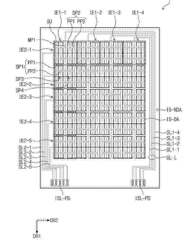
Resumen de: US2024288977A1
An input sensor including a first electrode and a second electrode, which cross each other. The first electrode includes a first main portion extending in a first direction and first sensing portions and second sensing portions, which are disposed with the first main portion therebetween in a second direction and each of which extends from the first main portion. Each of the first sensing portions and the second sensing portions includes first sub-portions extending in the first direction and first middle portions disposed between the first sub-portions and between one of the first sub-portions and the first main portion.
Nº publicación: WO2024174813A1 29/08/2024
Solicitante:
TSINGHUA UNIV [CN]
\u6E05\u534E\u5927\u5B66
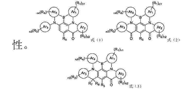
Resumen de: WO2024174813A1
The present invention relates to an organic compound, and also relates to the use of the organic compound in an organic electroluminescent device. The organic compound of the present invention has a structure as represented by formula (1), formula (2) or formula (3), or a structure formed by polymerizing any two of formula (1-1), formula (1-2), and formula (1-3). The organic electroluminescent device, which uses the compound of the present invention, has excellent device performance and stability.
 BOPI
BOPI
 Sede Electrónica